win2010
Member level 1

- Joined
- Sep 30, 2010
- Messages
- 35
- Helped
- 0
- Reputation
- 0
- Reaction score
- 0
- Trophy points
- 1,286
- Activity points
- 1,605
Hi..........
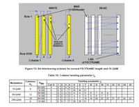
I attached image of DVB-T2 "Bit-Interleaver" in that columns and Rows are given. This is for 16-bit QAM and length is 64800-bits. This divided into 8100 rows and 8 columns. The data coming from previous block is "one Bit per Cycle". First bit store in 0th location like that First 8100 bits should store and later shift these bits circularly(ROTATE) according a "twisting parameter tc" listed in table below. Next 8100 also twist and store...so on up to 8 columns...
Write into Buffer(storage) as ROW wise:-
input indexs: 0 1 2 3 4 5 6 .... 8099
after circular 0 1 2 3 4 5 6 .... 8099
shitf using "tc=0"
if "tc=2" then 0 1 2 3 4 5 6 .... 8099
.................8099 8098 0 1 2 3 4 5 ...8097
this is upto 64800 bits and Reading(output) these twisted bits as column wise..like 0th location bit first,8099th second,serillaty 16199,24298,32397,40496,48595,56694,64793, 1, 8100, 16200...so on.....
I design using signal and variables in VHDL which is not synthesizing....
help me what best way of implimentation....

