Continue to Site

Welcome to EDAboard.com

Welcome to our site! EDAboard.com is an international Electronics Discussion Forum focused on EDA software, circuits, schematics, books, theory, papers, asic, pld, 8051, DSP, Network, RF, Analog Design, PCB, Service Manuals... and a whole lot more! To participate you need to register. Registration is free. Click here to register now.

How to go from a PN sequence expression to a block diagram ?

Status
Not open for further replies.

raka200

Member level 2
Joined
Aug 2, 2007
Messages
48
Helped
2
Reputation
4
Reaction score
0
Trophy points
1,286
Activity points
1,625
Hi everybody !!!!

Does anyboy could explain me how to go from a PN sequence expression to the block diagram ???
For example, in ATSC, there is a PN511 sequence used for the sync field segment.
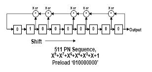
The expression for this sequence is X9+X7+X6+X4+X3+X+1

I thought we have to build a 9 taps shift register, and xor the taps 9,7,6,4,6,3,1 with '1', then barrel shift left (9 tap is oldest).
But the hardware implementation seems (to me ;-)) very different to the expression....
62_1186561063.jpg

Could someone tell me how to get from the sequence expression to the block diagram ????

Thank !
 

Re: PN sequence

The feedback shift register is going to generate the sequence:

s0 s1 s2 s3 s4 s5 s6 s7 s8 s9 s10 s11 s12 s13 ...

The register is preloaded with the first 9 values of the sequence like this:

[s8][s7][s6][s5][s4][s3][s2][s1][s0]--------> output

When the register outputs s0 by shifting right, s9 must be inserted in the position vacated by s8. The polynomial is a compact way of telling you how to calculate s9 from the previous values of the sequence. Basically it says that the modulo-2 sum of s9, s7, s6, s4, s3, s1 and s0 should be 0, or equivalently (given addition and subtraction are the same modulo-2):

s9 = s7 + s6 + s4 + s3 + s1 + s0

where the sum is implemented by a chain of mod-2 adders (exclusive-or gates if you like). I hope the link between the form of the polynomial and the expression just given is clear: s0 is in the sum because x^0 (i.e. 1) is in the polynomial; s1 is in the sum because x^1 is in the polynomial and so on. I hope too the link between the expression for s9 and the hardware is clear: there are taps at the register elements which contain s0, s1, s3, s4, s6 and s7 because their sum produces the feedback bit s9.

Of course, once you are told how to compute s9 the values for the remainder of the sequence are established by the same pattern, for example:

s10 = s8 + s7 + s5 + s4 + s2 + s1

Hope that helps.

David
 

    raka200

    Points: 2
    Helpful Answer Positive Rating
PN sequence

Hi
the output is related to "1" in "X9+X7+X6+X4+X3+X+1" and the left connection is related to "X9" in "X9+X7+X6+X4+X3+X+1"
 

Status
Not open for further replies.

Part and Inventory Search

Welcome to EDABoard.com

Sponsor

Back
Top