Continue to Site

Welcome to EDAboard.com

Welcome to our site! EDAboard.com is an international Electronics Discussion Forum focused on EDA software, circuits, schematics, books, theory, papers, asic, pld, 8051, DSP, Network, RF, Analog Design, PCB, Service Manuals... and a whole lot more! To participate you need to register. Registration is free. Click here to register now.

how to give waveport and air box for monopole antenna in hfss

Status
Not open for further replies.

dreamzalive

Junior Member level 1
Joined
Apr 20, 2011
Messages
18
Helped
0
Reputation
0
Reaction score
0
Trophy points
1,281
Activity points
1,406
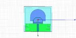
i am designing a uwb monopole antenna of substrate dimension 34x36 mm. i want yo know how to give the dimension of waveport and air box in hfss?my feedline is of width 3mm. it's 2 sidede antenna.
 

hi
your question is not clearly u mean CPW antenna ???????
 
it's an ultrawideband antenna. in this the patch is on one side of fr4 substrate of thickness 1mm and the ground is on the other side. patch consist of a semicircular area of radius 11mm,2 rectangles of 22x6mm and 14.1x3.7. feedline is a rectangle of 11.4x3 mm. on the other side ground is of dimension 11.2x36 mm. each is perfect e. it is a defected ground structure, a semi octagonal resonant ring on the back side of the antenna and an omega-shaped slot on the radiating patch.
�shaped slot on the radiating patch
 
Last edited:

hi
i think u antenna is small ground kind antenna so u can use lump port between your ground to feed line with same width by your feed line
 
and what should be the dimension of air box..a outlay of the antanna is attached. plz see...
 

Attachments

  • a.jpg
    a.jpg
    78.8 KB · Views: 194
Last edited:

hi
the radiation box with length of 80 mm is OK for this but u encountered with one or two problem when u simulated in fast mode for 2-18GHz (i never done with other method for UWB antenna ) if u done it for 3.1-10.6 or 2-12 it may be not appear
 
thanks for the reply..
80mm cube or 80 mm distance from the substrate on all side?? the problem is that i have to get notch at 3.3-3.6, 5.25-5.35 and 5.75-5.85 but i am getting at 3.2-3.8,4.7-5.0 and 5.5-5.7. i just have to shift 2nd and third notch that's all.
 

Hello,

No matter what antenna you are designing and for which frequency range it is,the general rule for air box dimension is that it should be Lamda/4 away from your radiating structure(antenna).In your case you are designing UWB antenna which operates from 3.1 to 10.6 GHz range so dont forget to use the Lamda calculated on the basis of lower operating frequency which in your case is 3.1 Ghz or 3GHz.
Your 2nd question,as said earlier use lumped port for excitation because it suits well for microstrip line feed.

Do correct your box size according to the rule mentioned above and if you still didnt get the results which you are expecting as mentioned in your last post above. Post your project and i will correct it for you.
/SC
 
thanks for ur help...it was really very helpful. attached file is the paper which i want to implement on fr4. the paper is on rtduroid. in fr4 it is not giving the proper notch as well the notch is also at the wrong place. using lambda=12.255 i.e lambda/4 only two notches are coming. i don't know how to upload hfss project. so please help me out.
 

Attachments

  • antenna (2).pdf
    942.2 KB · Views: 257

i am using lumped port of dimension 3x3 mm
 

Hi,

i had a quick look through the paper you have uploaded. Have you optimized the width of your microstrip feedline according to FR4 subtrate to achieve 50ohms characteristic impedance??? If you are using the same dimension of 2.84mm as specified in the paper then its wrong because they have calculated it according to the substrate they have used which is RTduroid. For the microstrip dimensions you can take help from pozar book of microwave engineering or check the following calculator

Microstrip Line Calculator | em: talk

Using it correct your microstrip feedline dimensions and i am sure your problem will be solved.you have to use lumped port of same dimension as that of your microstrip feedline width and substrate height.

If you have correct dimensions of microstrip feed line and above mentioned things are already taken care of then i am not sure whats wrong with your project. I cant help you untill and unless i see your project to know what you are doing. Upload your project and i ll have a look at it.

/SC
 

    V

    Points: 2
    Helpful Answer Positive Rating
could you please tell me how to upload the project??

---------- Post added at 17:04 ---------- Previous post was at 15:07 ----------

i have done every thing as given in paper only,except my feedline which is of width 2mm.
my port is of width 2mm and height 1mm. i am getting a notch at 2.8-3.6, 4.8-5.2 and 5.4-5.6. i am using the air boundary of 12.255 from each surface. plz tell me what is wrong in this as i am not getting the proper result and also my 2nd and third notch has vswr of around 2.5.

---------- Post added at 17:16 ---------- Previous post was at 17:04 ----------

and also all my surfaces are perfect-e
 

t23 is with air box lambda/4 and the other one is the closest i am getting. plz see this
 

Attachments

  • 3ghzlumped3x3.rar
    13.5 KB · Views: 137
  • t23.rar
    13.6 KB · Views: 137

i also tried by the wave port dimension 11.4x2 mm to get characteristic impedence of 50ohm but the result was not desirable....
 

hi i design many antenna hfss but for some kind of antenna i used wave port usually its not as well as u want but in CST wave port better than lump port
u simulation have some problem i repaired them for but i cant understand why u change substrate ?
 

Attachments

  • t23.zip
    16.4 KB · Views: 123
thanks for your help.
actually i wante to fabricate this antenna and since fr4 is a lot cheaper than the rt-duoroid i went for fr4. but i was not getting the proper notch.
in this file i m hetting notches at 3.2-3.6, 4.5-4.9 and 5.4-5.6 in comparison of 3.3-3.6,5.2-5.35, 5.75-5.85. can you please tell me how can i get that. should i decrease the feedline to 2mm instead of 3 in order to get characteristis impedence of 50ohm..
 
Last edited:

hi
u cant get good result because FR4 loss is to much and it cant work as well as other material but i check and try for u
 

really, thanks for your help. i really appreciate it.
 

Hi,

See the attached file i have corrected it. The first Notch is exactly at the same frequency range as desired,the second is a little earlier from 5.01-onwards. The notches have relatively low VSWR because FR4 is a lossy material and above 1GHz losses of FR4 gets high and that is the reason 3rd Notch is not even appearing. Apart from this Feedline width is not correct for 50Ohms,it should be around 1.9mm to achieve 50Ohms characteristic impedance. How you have decided for 3mm width???? Any special reason???? Your Airbox size wasnt correct as Lamda/4 is 25mm not 12.5mm if you calculate Lamda using f=3Ghz your Lumped port excitation was defined for 36Ohms,i dont know why. I have corrected it for 50Ohms aswell. You have changed the substrate so microstrip feedline width ll be changed and accordingly all other dimensions will change in order to get the same exact results of the paper you have mentioned.

My suggestion: Use the same substrate as specified in Paper and try to replicate the results of the paper by using exact dimensions mentioned in paper. That is always the first step. Once it is done,then you can change the substrate to FR4 or any desired material and then see its effects on the result. In order to maintain the same results you can play with dimensions of different parts of antenna geometry. I hope you have got my point.

/SC
 

Attachments

  • t23.rar
    39.6 KB · Views: 141
Status
Not open for further replies.

Part and Inventory Search

Welcome to EDABoard.com

Sponsor

Back
Top