Continue to Site

Welcome to EDAboard.com

Welcome to our site! EDAboard.com is an international Electronics Discussion Forum focused on EDA software, circuits, schematics, books, theory, papers, asic, pld, 8051, DSP, Network, RF, Analog Design, PCB, Service Manuals... and a whole lot more! To participate you need to register. Registration is free. Click here to register now.

How to find desired AC Voltage Source and Ground Symbol Using KiCAD

Status
Not open for further replies.

narayani

Full Member level 2
Joined
Aug 15, 2014
Messages
120
Helped
0
Reputation
0
Reaction score
1
Trophy points
1,298
Activity points
2,262
I am using the KiCAD software for drawing schematics, I have searched the desired symbols for AC Voltage Source and Ground using KiCAD software, I couldn't find the desired symbols of AC Voltage Source and Ground.
Can you help me to find the desired symbols of AC Voltage Source and Ground in the KiCAD software.
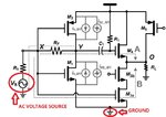
Desired AC Voltage Source and Ground symbols is shown in the below screen shot schematic.
 

Attachments

  • Schematic_Showing_AC_Voltage_and_Ground.jpg
    Schematic_Showing_AC_Voltage_and_Ground.jpg
    58.6 KB · Views: 658

Desired symbols of AC voltage and Ground as shown in the posting #1 screen shot is it available in the KiCAD. Can you someone help me to get those symbols using KiCAD.
 

Make them yourself....
How to make, I don't know, I am beginner, can you help me to create myself desired AC Voltage Source and Ground using KiKAD. Which option I have to use and Where I have to go and get for Circle and lines and tidle symbols. Please help me.
 

So much to learn ... So little time.. When you do find/create the symbol, add a source resistance.

**broken link removed**

http://wiki.xtronics.com/index.php/Eeschema


This presents some problems - if you want to keep the grounds separated, (lets say to control noise induced by ground currents) then you can make your own part versions with non-power-port pins (flag "Power Symbol" must be cleared (In libedit, Part Properties/Options).
Some parts call ground pins GND while others may have it as VSS - you can connect them with power symbols for these names. There is some other foot work needed with the use of a PWR_FLAG to prevent ERC from detecting them as unpowered.
Best Practice It is popular to not bring out the power pins on parts - and let power be automatic, this practice might save time, but at the cost of failing to communicate what is going on. A better way.
Create separate power units for logic chips and opamps and put them and their associated bypass caps below the main circuit. This helps to show which bypass-cap is intended for which chip. It also suggests that the bypass needs to be close to the chip it is bypassing.
Don't use invisible power pins. Current flowing on ground returns create voltages - seeing the power connections helps prevent noise problems.
FWIW

http://kicad.rohrbacher.net/quicklib.php
 
Sir,
I am feeling really difficult to draw my own symbols using KiCAD. I tried to draw circle and my own ground as shown in the posting #1. I could achieved the ground as shown in the Posting #1, but How to save this and transfer to main schematic this ground symbol, I am facing problem.
I have also drawn circle for AC SOURCE, but I don't know how to draw tidle sign inside cirlce using KiCAD, I am not getting. Once we draw the Circle and tidle sign inside the circle for AC source and ground symbol. How to save these symbols and and how to use these symbols, where we require, Can you some body help me.
 

Attachments

  • KiCAD_Library_Editor.jpg
    KiCAD_Library_Editor.jpg
    117.7 KB · Views: 221

If you read my first link.....
It is time to place the power and ground symbols. Click on the 'Place a power port' button right toolbar. Alternatively, press the on the a key and choose the 'power' library. In the component selection window, click on the 'List All' button. Scroll down and select 'VCC' from the Select Component window. Click OK. 27. Click above the pin of the 1k resistor to place the VCC part. Click on the area above the microcontroller 'VDD'. In the 'Component Selection history' section select 'VCC' and place it next to the VDD pin. Repeat the add process again and place a VCC part above the VCC pin of 'MYCONN3'. 28. Repeat the add-pin steps but this time select the GND part. Place a GND part under the GND pin of 'MYCONN3'. Place another GND symbol on the right of the VSS pin of the microcontroller. Your schematic should now look something like this
 
You may want to subscribe to Yahoo help forum on KIcad

http://groups.yahoo.com/group/kicad-develYahoo! Groups Links

<*> To visit your group on the web, go to:
https://groups.yahoo.com/group/kicad-users/

<*> Your email settings:
Individual Email | Traditional

<*> To change settings online go to:
https://groups.yahoo.com/group/kicad-users/join
(Yahoo! ID required)

<*> To change settings via email:
kicad-users-digest@...
kicad-users-fullfeatured@...

Please read the Kicad FAQ in the group files section before posting your question. Please post your bug reports here. They will be picked up by the creator of Kicad.

Although I cant wait to see how your board layout connection to a generator looks :laugh:...just kidding. What Kicad wont import images or allow ASCii? (~)—:bang:
 

Status
Not open for further replies.

Part and Inventory Search

Welcome to EDABoard.com

Sponsor

Back
Top