Continue to Site

Welcome to EDAboard.com

Welcome to our site! EDAboard.com is an international Electronics Discussion Forum focused on EDA software, circuits, schematics, books, theory, papers, asic, pld, 8051, DSP, Network, RF, Analog Design, PCB, Service Manuals... and a whole lot more! To participate you need to register. Registration is free. Click here to register now.

How to figure out cutoff frequency using scope for LC filter post SMPS

Status
Not open for further replies.

witssq

Junior Member level 1
Joined
Mar 22, 2009
Messages
16
Helped
0
Reputation
0
Reaction score
0
Trophy points
1,281
Activity points
1,407
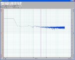
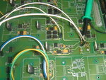
I am using commercial SMPS +5, +/-5V output.


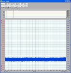
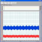
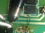
Against SMPS output, I applied LC filter, and achieved 45mV noise down to 20mV noise, but I need about 5mV or below.


Please anyone help me about how to find cutoff frequency not easy to figure out


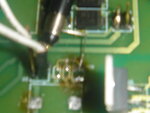
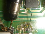
The microscopic view is after currently filtered.


Best regards,

SunSung
 

Attachments

  • B_1.JPG
    B_1.JPG
    246.3 KB · Views: 122
  • B_2.JPG
    B_2.JPG
    189.7 KB · Views: 111
  • Doc.zip
    429.8 KB · Views: 93

You have 2 options, decrease the bandwidth of filter or increase the order of the filter. As you said you need 12 dB more rejection. Simply, increase the order of filter from 2 to 4.
 

Thanks for your response.

The current test schematic is attached.
Test result is as follows,
TP1 noise 45mV(Peak to Peak)
TP2 noise 23mV(Peak to Peak)
TP3 noise 16mV(Peak to Peak)
TP4 noise 15mV(Peak to Peak)

The change on 2 order to 4 order seems to be little effect on ripple after testing.

Please advice about that the passive component values is correct and how I would approach my goal.


Best regards,
 

Attachments

  • POwer.zip
    353.6 KB · Views: 96
Last edited:

1.What is the frequency of switching and let say we confined ourselves to use a second order LC filter. H(s)=1/(1+(s/wo)^2) in which W0=1/sqrt(LC). Assume that the switching frequency is much further that wo. then the rejection of it can be found by :

Attenuation=(Wswitch/W0)^2. you like to decrease 45mv to 2mV. ==> Wswitch/W0=sqrt(45/2)=4.7. So just for being more sure W0=0.1*Wswitch. From this you can find the LC product. If the value of L and C are very big and you like to decrease them, you just need to increase the switching frequency of the circuit.

At the end and after designing the filter, you may need to add small resistor in series with inductor to reduce the ringing due to the filter itself.

Conclusion: Just increase the Value of L and C of the filter to reduce the ringing.
 

The spectrum plot raises doubts, that the shown voltage level is actually generated from the SMPS, because effectively no discrete lines are visible. It looks rather like amplifier noise or another kind of measurement artefacts. Thus the measurement seems unsuitable to determine a filter dimensioning.

P.S.: Also the shown numbers for interference levels sound unreasonable considering the given circuit. Apparently, the probed voltage is almost unaffected by the LC filters. This isn't a problem of filter dimensioning rather than probe connection or possibly circuit ground layout.
 
Last edited:

Except LC filtering, you have regulator( Active filtering), which can diminish the ripples on the power supply. As you see by it's AC gain, after 1MHz, the regulator hardly can diminish the high frequency noises.Also, increase the accuracy of the simulator.
 

Many thanks for your responses.

I will immediately return more accurate results.

The spectrum plot raises doubts, that the shown voltage level is actually generated from the SMPS, because effectively no discrete lines are visible. It looks rather like amplifier noise or another kind of measurement artefacts. Thus the measurement seems unsuitable to determine a filter dimensioning.

P.S.: Also the shown numbers for interference levels sound unreasonable considering the given circuit. Apparently, the probed voltage is almost unaffected by the LC filters. This isn't a problem of filter dimensioning rather than probe connection or possibly circuit ground layout.

You are correct. The attached spectrum result is at final stage (at Test Point 4 on shematic).
Please notify if you know materials about accurate probing.

Best regards,

---------- Post added at 06:02 ---------- Previous post was at 05:38 ----------

1.What is the frequency of switching and let say we confined ourselves to use a second order LC filter. H(s)=1/(1+(s/wo)^2) in which W0=1/sqrt(LC). Assume that the switching frequency is much further that wo. then the rejection of it can be found by :

SMPS is commercial product. Requesting manufacturer, they say that 10KHz - 60KHz as to load.
 

Thanks for your interests.

I increased LC filter value between TP1 and TP2, 1mH and 10uF, but I cannot find significant change on noise figure. and 4 order with same values made more fluctuation than before.

The TP1 and TP2 test graph is attached.

Please let me know about the detailed procedure to how I could cleary quantify this problem.

P.S.: Also the shown numbers for interference levels sound unreasonable considering the given circuit. Apparently, the probed voltage is almost unaffected by the LC filters. This isn't a problem of filter dimensioning rather than probe connection or possibly circuit ground layout.

for the above comment could you explain me the details, if not available, please
advise me a material.

Best regards,
SunSung
 

Attachments

  • Power_Reg2.JPG
    Power_Reg2.JPG
    194.5 KB · Views: 101

could you explain me the details
I think, the "noise" level measured after the voltage regulator doesn't show a signal that is propagated through the filter and regulator. I assume, that it either shows a measurement artefact (e.g. due to incorrect probe grounding) or interferences that bypass the filter, because the circuit layout is unsuitable.
 

Hi, FvM and Milad-D

I think that before more thing to do what you said, the first thing I shoud do is
improve measurement accuracy.

So, I tested referring to the material **broken link removed**.
As you see the attached image. I measure ground voltage on PCB with probe with sprung earth-tip. The result is 3mV ripple. And, when I directly (not on the PCB) measured scope ground, the result is similar.

And when I measure at TP2, the reult is 16mV(scope range set 1ms/DIV), but TP3, TP4 ripple is similar.

My scope datasheet is attached.

Before I do more things to do you suggested, do you think about more works to
improve measurement accuracy and against artifacts.

If I should do more things for measurement, please advise me.

Because I think that test result could be useless without reasonalbe measurement accuracy,
after this step, I would like to test your suggestions.

Please give me advice.

Best regards,
SunSung
 

Attachments

  • Cleverscope Data Sheet.pdf
    266.6 KB · Views: 90
  • DSC08157.JPG
    DSC08157.JPG
    1.2 MB · Views: 112
  • DSC08158.JPG
    DSC08158.JPG
    1.2 MB · Views: 107
  • DSC08159.JPG
    DSC08159.JPG
    1.2 MB · Views: 104
  • DSC08160.JPG
    DSC08160.JPG
    1.1 MB · Views: 112

Hi, Milad-D

Please let me know about details about your saying
As you see by it's AC gain, after 1MHz, the regulator hardly can diminish the high frequency noises
.
What do you mean as AC gain, after 1MHz(How do you figure out 1MHz).

Best regards,
SunSung
 

I see, that the PCB is rather complex. In my opinion, it's necessary to understand the interference sources and pathes of spreading.

Using short bayonet ground tips is basically good, but common mode interferences can also spread through the probe cable. To determine the probe interference level, you may want to measure the voltage between two adjacent ground pads with the same method. If it's neglectable, you can trust the measurements.

I understand that Milad-D is referring to the ripple rejection specification of the regulator. It's low at high frequencies, but still about 20 dB. So the output "noise" level should be lower by a factor of 10. The fact, that it isn't raises doubts about signifance of the measurements.
 

Hi, FvM

Thanks for response.

To determine the probe interference level, you may want to measure the voltage between two adjacent ground pads with the same method. If it's neglectable, you can trust the measurements.
As I noted, I measure near ground pad with below 1 inch(maybe below 10mm), The result is 3mV. Could I trust measuring result. Is that not negligible?

Best regards,
SunSung
 

Could I trust measuring result. Is that not negligible?
Sorry, I missed the respective explanation in your previous post. Yes, I think 3 mV is acceptable. The interference spreading mechanism in your circuit is still unclear to me.
 

Thanks for your response.

The interference spreading mechanism in your circuit is still unclear to me
Please kindly explain me about what interference spreading mechanism means.

Best reagrds,
SunSung
 

Status
Not open for further replies.

Similar threads

Part and Inventory Search

Welcome to EDABoard.com

Sponsor

Back
Top