Continue to Site

Welcome to EDAboard.com

Welcome to our site! EDAboard.com is an international Electronics Discussion Forum focused on EDA software, circuits, schematics, books, theory, papers, asic, pld, 8051, DSP, Network, RF, Analog Design, PCB, Service Manuals... and a whole lot more! To participate you need to register. Registration is free. Click here to register now.

How to determine the passband attenuation, stop-band rejection, and passband ripple

Status
Not open for further replies.

bhl777

Full Member level 6
Joined
Sep 30, 2008
Messages
363
Helped
0
Reputation
0
Reaction score
0
Trophy points
1,296
Activity points
5,140
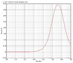
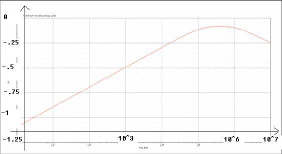
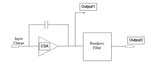
Hi guys, I designed a OTA-C bandpass filter according to some spec. from a supervisor. The pictures are the Cadence simulation of the bandpass performance. But I do not know how to use this data to determine the specs of this filter, like (1) passband attenuation, (2) stop-band rejection, and (3)passband ripple.
If I want to say the passband is from 100Mhz to 1Ghz, does any one tell me how to calculate those parameters?
 

Attachments

  • 1.jpg
    1.jpg
    51.3 KB · Views: 208

There are several comments to be made:
* The passband is in the 100 kHz range (not MHz)
* Passband and stopband attenuation can be determined only if you know (and tell us) about the passband and stopband frequencies.
* passband ripple (if any!) cannot be detected because of bad frequency resolution. You need more calculated points of the transfer curve.
* You should use logarithmic scales for both axes (dB) and display alos the phase .
 
  • Like
Reactions: bhl777

    bhl777

    Points: 2
    Helpful Answer Positive Rating
Hello LvW,thank you for your guidance and I uploaded the db plot (only the magnitude but not phase yet). Yes you are right, I made a mistake for saying the passband. So for this case, could you tell me (1) how can I caculate Passband and stopband attenuation if I want the passband is from 1KHZ to 100 khz?
(2) Could you also tell me for analog IC filter, what kind of value regarding passband attenuation and stopband rejection is acceptable? Then I can revise the circuit to meet this value.
(3) Could you tell me that from this picture is it able to find out some points to calculate passband ripple? Because I have no idea of this and want to know if there is any requirement for analog circuit to have a specific range. Please advise and I appreciate you very much!


There are several comments to be made:
* The passband is in the 100 kHz range (not MHz)
* Passband and stopband attenuation can be determined only if you know (and tell us) about the passband and stopband frequencies.
* passband ripple (if any!) cannot be detected because of bad frequency resolution. You need more calculated points of the transfer curve.
* You should use logarithmic scales for both axes (dB) and display alos the phase .
 

*At first, I suppose your bandpass is of 2nd order.
In this case, the passband is mostly defined between the two frequencies for which the gain is 3dB less than the maximum gain.
In your case this would be app. a level of -3.1 dB on both sides of the maximum. However, this region is not shown in your diagram.
*According to your diagram the passband attenuation is 0.1 dB.
*Passband ripple exist only for bandpass functions of higher order (4, 6,...).
*The task of a bandpass is to attenuate some freqency components outside the passband. For these frequencies the stopband attenuation is defined. Do you have any requirenents in this respect?

---------- Post added at 15:20 ---------- Previous post was at 15:17 ----------

By the way: Is it the same filter as in your 1st posting?
 
  • Like
Reactions: bhl777

    bhl777

    Points: 2
    Helpful Answer Positive Rating
Hello LvW, thank you for your guidance. I am new to the filter design and still confused of some specs.
(1)Thank you for telling me that passband ripple only exists for higher order. Yes my filter is 2-order, so there is no ripple, thank you for this instruction!
(2) You said -3.1db, do you mean from the top of the plot, it is around -0.15? Is it OK for a filter?
(3) Now I just want to present this filter as a project work (not have a specification already and tried to meet it), so I need to define a passband range (like from f1 to f2). How can I define the range from the plot and present that in this range the filter works well?
(4) After you define the range from the plot, could you tell me how to calculate the stopband rejection accroding to its db?


*At first, I suppose your bandpass is of 2nd order.
In this case, the passband is mostly defined between the two frequencies for which the gain is 3dB less than the maximum gain.
In your case this would be app. a level of -3.1 dB on both sides of the maximum. However, this region is not shown in your diagram.
*According to your diagram the passband attenuation is 0.1 dB.
*Passband ripple exist only for bandpass functions of higher order (4, 6,...).
*The task of a bandpass is to attenuate some freqency components outside the passband. For these frequencies the stopband attenuation is defined. Do you have any requirenents in this respect?

---------- Post added at 15:20 ---------- Previous post was at 15:17 ----------

By the way: Is it the same filter as in your 1st posting?
 
Last edited:

(1)Thank you for telling me that passband ripple only exists for higher order. Yes my filter is 2-order, so there is no ripple, thank you for this instruction!
If you want you can see the gain variation within the passband as ripple (some people do that). See (2) below.

(2) You said -3.1db, do you mean from the top of the plot, it is around -0.15? Is it OK for a filter?

It is the normal case to specify the -3 dB points (below the maximum) as passband. However, depending on the application and the requitements, respectively, you also can define the passband for any other values.
Example: If you allow only a 0.1 dB variation within the passband (0.25-0.15 dB) , one can derive the following edge frequencies from your drawing: 20 kHz.....10 MHz. (By the way, that is very very broad!).
For other attenuation values you must extend the displayed frequency range.

(3) Now I just want to present this filter as a project work (not have a specification already and tried to meet it), so I need to define a passband range (like from f1 to f2). How can I define the range from the plot and present that in this range the filter works well?

See above. The answer, if it works "well" can be given only in case the requirements are known. But, as mentioned above, the bandpass seems to exhibit a very small quality factor Q (very large bandwidth).

(4) After you define the range from the plot, could you tell me how to calculate the stopband rejection accroding to its db?

As mentioned earlier: What are the stopband frequencies?

Some general remarks (perhaps helpful):
Normally, a bandpass and its parameters are defined as follows:
1.) The bandpass center frequency is fo=...Hz. The gain or attenuation at fo shall be ...dB
2.) The filter must transfer frequencies between f1 and f2 (passband) ; the gain/attenuation in this region must not vary by more than x dB (example 1 or 3 dB).
3.) The following frequencies f<f3 and f>f4 must be attenuated at least by y dB (example 60 dB). This defines the stopband frequencies.

Regards, LvW
 
Last edited:
  • Like
Reactions: bhl777

    bhl777

    Points: 2
    Helpful Answer Positive Rating
Hello LvW, thank you for your kindest help. I just found that you also asked me if the two plots I put are for the same filter. The answer is YES!

Regarding your answers, I still have some confusion and hope you can help me out.

(1) Your explanation of passband and stopband is very clear. As you said, the center frequency will be around 500Khz and the frequency is between 20Khz and 10Mhz. But for the ranges outside it, I cannot reach like -60db. If even in 1HZ, the attenuation is still not -60DB, does it mean that this bandpass filter is not good?

(2) If the Q is small, does it mean that the performance is not good? The transfer fucntion is (Gm/C)/{s+(Gm/C)}, could you tell me how to calculate Q from this equation?

(3) I saw an application of bandpass filter and try to understand it. Could you have a look at the attachment? A step down signal goes into the charge sensitive amplifier, then it went out with a step down signal. Then this step down signal goes into the bandpass filter and comes out with another shape. What is the function of the bandpass filter here? Because I think that either step up or step down signal has no specific frequency, why it should be applied to the bandpass filter?
2.jpg

Thank you very much!

(1)Thank you for telling me that passband ripple only exists for higher order. Yes my filter is 2-order, so there is no ripple, thank you for this instruction!
If you want you can see the gain variation within the passband as ripple (some people do that). See (2) below.

(2) You said -3.1db, do you mean from the top of the plot, it is around -0.15? Is it OK for a filter?

It is the normal case to specify the -3 dB points (below the maximum) as passband. However, depending on the application and the requitements, respectively, you also can define the passband for any other values.
Example: If you allow only a 0.1 dB variation within the passband (0.25-0.15 dB) , one can derive the following edge frequencies from your drawing: 20 kHz.....10 MHz. (By the way, that is very very broad!).
For other attenuation values you must extend the displayed frequency range.

(3) Now I just want to present this filter as a project work (not have a specification already and tried to meet it), so I need to define a passband range (like from f1 to f2). How can I define the range from the plot and present that in this range the filter works well?

See above. The answer, if it works "well" can be given only in case the requirements are known. But, as mentioned above, the bandpass seems to exhibit a very small quality factor Q (very large bandwidth).

(4) After you define the range from the plot, could you tell me how to calculate the stopband rejection accroding to its db?

As mentioned earlier: What are the stopband frequencies?

Some general remarks (perhaps helpful):
Normally, a bandpass and its parameters are defined as follows:
1.) The bandpass center frequency is fo=...Hz. The gain or attenuation at fo shall be ...dB
2.) The filter must transfer frequencies between f1 and f2 (passband) ; the gain/attenuation in this region must not vary by more than x dB (example 1 or 3 dB).
3.) The following frequencies f<f3 and f>f4 must be attenuated at least by y dB (example 60 dB). This defines the stopband frequencies.

Regards, LvW
 

Attachments

  • 2.jpg
    2.jpg
    11.7 KB · Views: 74
Last edited:

Some additional comments:
The transfer function is (Gm/C)/{s+(Gm/C)}, could you tell me how to calculate Q from this equation?
It's a 1st order lowpass rather than a bandpass transfer function. It has a real pole, for which no Q can be determined.

Your original frequency response is showing a second order bandpass, as said. But for high relative bandwidth/low Q, it can be better represented as a lowpass/highpass combination. If you want to improve the stop band attenuation, you can increase the lowpass and/or highpass order without changing the bandwidth.

P.S.: It's difficult to guess about the purpose of the bandpass following the charge amplifier without knowing about the involved signal. It can be e.g. a means to improve the signal-noise ratio or just a special preprocessing required by the succeeding signal chain. A possible application would be e.g. a nuclear particle detector with pulse height discrimination or energy spectrum measurement.

Strictly spoken, the charge amplifier output can't be a step function, because a real amplifier needs a time constant to reset the integrator. Otherwise, it can't process repeated input events.
 
Last edited:
  • Like
Reactions: bhl777

    bhl777

    Points: 2
    Helpful Answer Positive Rating
Hello LvW, thank you for your kindest help. I just found that you also asked me if the two plots I put are for the same filter. The answer is YES!

*The bandpass transfer curve in your 1st posting #1 exhibits a 3-dB bandwidth (70.7% of the maximum level) between
f1=100 kHz and f2=1.5 MHz.

* Question: Which expression is plottet against the frequency in posting#3 ? Up to now, I was of the opinion it is the magnitude in dB. But this is not the case if both plots originate for the same filter.

Please clarify.
 
  • Like
Reactions: bhl777

    bhl777

    Points: 2
    Helpful Answer Positive Rating
Hello FvM, thank you so much for your reply!
(1)I am terribly sorry that I made the mistake. The transfer function is [(Gm/C)/{s+(Gm/C)}]×[1/{s+(Gm/C)}]. Yes in the real circuit I connect a lowpass with a highpass. Could you show me how to calculate Q for this transfer fucntion?
(2)You said that it can be better represented as a lowpass/highpass combination, and I am curious that is it any differences between lowpass/highpass combination and bandpass? Because from the textbook I saw that bandpass is lowpass/highpass combination, please advise!
(3)You mentioned that the charge amplifier output can't be a step function, can I understand that you are talking about some settling time to be stable, which means there is a slope for the output to go from 0 to "1" (the specific value)?
(4)Could you tell me more about charge sensitive amplifier? I am not talking about this case but just want to know some more general about CSA. Does it mean that output voltage of CSA is proportional with input charge? For example,
I suppose the input of CSA is a current signal I=k(t-t1), then the total integral of the current during time t is the charge, if we have a capacitor which connects with the CSA in parallel (like the picture I posted above), and the output of the CSA a voltage which is proportional to t^2. So Vout is proportional with Qin, is it correct?
(5) If I want to treat the bandpass filter as a peak detector, do you think is it correct? I mean the peak value of the output is proportional to the input of the filter, and eventually proportional with the input charge, is it a reasonable model?
I appreciate you so much and feel so lucky to get the guidance from you and LvW!
Some additional comments:

It's a 1st order lowpass rather than a bandpass transfer function. It has a real pole, for which no Q can be determined.

Your original frequency response is showing a second order bandpass, as said. But for high relative bandwidth/low Q, it can be better represented as a lowpass/highpass combination. If you want to improve the stop band attenuation, you can increase the lowpass and/or highpass order without changing the bandwidth.

P.S.: It's difficult to guess about the purpose of the bandpass following the charge amplifier without knowing about the involved signal. It can be e.g. a means to improve the signal-noise ratio or just a special preprocessing required by the succeeding signal chain. A possible application would be e.g. a nuclear particle detector with pulse height discrimination or energy spectrum measurement.

Strictly spoken, the charge amplifier output can't be a step function, because a real amplifier needs a time constant to reset the integrator. Otherwise, it can't process repeated input events.
 

I don't know, which text book you are referring to. In my view, a passive RLC circuit or an equivalent active "resonator" circuit would be considered as the common 2nd order bandpass prototype. For low Q, the complex pole pair turns however into two real poles and the bandpass can be represented by separate low- and highpasses.

I fear, the CSA topic tends to go too far beyond the present thread's scope. The "output can't be a step function" point is simply referring to the fact, that the integrator must be reset either periodically by a switch or "continuously" by a resistor in parallel to the capacitor.
 
  • Like
Reactions: bhl777

    bhl777

    Points: 2
    Helpful Answer Positive Rating
(1)I am terribly sorry that I made the mistake.The transfer function is [(Gm/C)/{s+(Gm/C)}]×[1/{s+(Gm/C)}]

I am afraid, you again have made a mistake. The 2nd part of the function equals a 1st order highpass only when you replace the "1" by "s". OK?

(2)You said that it can be better represented as a lowpass/highpass combination, and I am curious that is it any differences between lowpass/highpass combination and bandpass? Because from the textbook I saw that bandpass is lowpass/highpass combination, please advise!

To realize a 2nd order bandpass you generally have two options:
(a) A combined frequency-selective LC or active RC combination that can produce a conjugate-complex pole pair (for high Qp and good selectivity), or
(b) A series combination of a 1st order lowpass with a 1st order highpass. In this case - as mentioned by FvM - you realize only two real poles (instead of complex) with rather poor selectivity (rather large bandwidth).
 
  • Like
Reactions: bhl777

    bhl777

    Points: 2
    Helpful Answer Positive Rating
Yes you are right!Thank you very much for your guidance LvW!
(1)I am terribly sorry that I made the mistake.The transfer function is [(Gm/C)/{s+(Gm/C)}]×[1/{s+(Gm/C)}]

I am afraid, you again have made a mistake. The 2nd part of the function equals a 1st order highpass only when you replace the "1" by "s". OK?

(2)You said that it can be better represented as a lowpass/highpass combination, and I am curious that is it any differences between lowpass/highpass combination and bandpass? Because from the textbook I saw that bandpass is lowpass/highpass combination, please advise!

To realize a 2nd order bandpass you generally have two options:
(a) A combined frequency-selective LC or active RC combination that can produce a conjugate-complex pole pair (for high Qp and good selectivity), or
(b) A series combination of a 1st order lowpass with a 1st order highpass. In this case - as mentioned by FvM - you realize only two real poles (instead of complex) with rather poor selectivity (rather large bandwidth).


---------- Post added at 13:16 ---------- Previous post was at 13:15 ----------

Thank you very much for your guidance Fvm!
I don't know, which text book you are referring to. In my view, a passive RLC circuit or an equivalent active "resonator" circuit would be considered as the common 2nd order bandpass prototype. For low Q, the complex pole pair turns however into two real poles and the bandpass can be represented by separate low- and highpasses.

I fear, the CSA topic tends to go too far beyond the present thread's scope. The "output can't be a step function" point is simply referring to the fact, that the integrator must be reset either periodically by a switch or "continuously" by a resistor in parallel to the capacitor.
 

Hello LvW, thank you for pointing out this problem! I am sorry that I just found this reply from you! There are some problems of the plots in #3. And I want to clarify with something and ask some more questions.
Let us focus on plot in #1.
(1)The input of the bandpass filter is 100mV. And the peak value of the output is around 400mV. So the magnitude was amplified. Is it OK for a filter to amplified the input?
(2) Is the peak db of the filter MUST be 0 or less than 0?
Thank you very much!!!!!!!!!!!!!!!!!!


Hello LvW, thank you for your kindest help. I just found that you also asked me if the two plots I put are for the same filter. The answer is YES!

*The bandpass transfer curve in your 1st posting #1 exhibits a 3-dB bandwidth (70.7% of the maximum level) between
f1=100 kHz and f2=1.5 MHz.

* Question: Which expression is plottet against the frequency in posting#3 ? Up to now, I was of the opinion it is the magnitude in dB. But this is not the case if both plots originate for the same filter.

Please clarify.
 

Hello LvW, thank you for pointing out this problem! I am sorry that I just found this reply from you! There are some problems of the plots in #3. And I want to clarify with something and ask some more questions.
Let us focus on plot in #1.
(1)The input of the bandpass filter is 100mV. And the peak value of the output is around 400mV. So the magnitude was amplified. Is it OK for a filter to amplified the input?
(2) Is the peak db of the filter MUST be 0 or less than 0?
Thank you very much!!!!!!!!!!!!!!!!!!

OK, it is good to know if a diagram like #1 shows an output voltage or the transfer function. Please note, that it is really important to explain what a diagram shows.
To your question (1): In many cases it is desired or even a requirement to have passband gain. In your case the maximum gain is 12 dB. Please note, that normally such a diagram should be scaled in dB on a logarithmic frequency axis.

Question (2): I don't understand. I think it is answered by (1), is it not?
 
  • Like
Reactions: bhl777

    bhl777

    Points: 2
    Helpful Answer Positive Rating
Hello LvW,thank you so much for your reply and instruction! Now I know about this and am very sorry for confusion I made for you. Yes actually when you answer question 1, the question 2 is also andwered. I appreciate that very much!
OK, it is good to know if a diagram like #1 shows an output voltage or the transfer function. Please note, that it is really important to explain what a diagram shows.
To your question (1): In many cases it is desired or even a requirement to have passband gain. In your case the maximum gain is 12 dB. Please note, that normally such a diagram should be scaled in dB on a logarithmic frequency axis.

Question (2): I don't understand. I think it is answered by (1), is it not?
 

Status
Not open for further replies.

Part and Inventory Search

Welcome to EDABoard.com

Sponsor

Back
Top