Continue to Site

Welcome to EDAboard.com

Welcome to our site! EDAboard.com is an international Electronics Discussion Forum focused on EDA software, circuits, schematics, books, theory, papers, asic, pld, 8051, DSP, Network, RF, Analog Design, PCB, Service Manuals... and a whole lot more! To participate you need to register. Registration is free. Click here to register now.

How to design this circuit??

Status
Not open for further replies.

zcs20060925

Newbie level 4
Joined
Oct 19, 2008
Messages
6
Helped
0
Reputation
0
Reaction score
0
Trophy points
1,281
Activity points
1,324
Hi, friends,
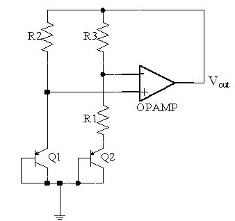
Can anyone tell me the steps of designing this bandgap below, assuming the desired specifications are given?
Must the mismatch between resistors and BJTs, the offset of OPAMP, the noise from all components be considered,during the design?
How to considered these nonideal impacts, and how to select the OPAMP?
More details are expected.....Thanks !!!!1[/img]
98_1260187431.jpg
 

Take OP-07 for the op-amp. They are ultra low offset voltage op-amps. Plus there is a dedicated setup built in it to reduce the effect offset and bias voltages down to uV or even less. (Refer to data sheet for details on this)

Pick up 'chip resistors' if you want extreme accuracy in their operation without any tolerance. They are pretty expensive but very good + they are in the form of array on the chip.

Same goes for transistors. Transistor arrays are available in the form of IC's. And those IC's are not quiet expensive.

My recommendation would be to install a voltage nullifying network for the op-amp and work with it to eliminate the offsets. And work with discrete resistors and transistors. They dont matter much. But dont work with them at above 30 deg C. Non-linear effects of transistor with temperature can be obtained from its data sheet.

Cheers.
 

khansaab21 said:
Take OP-07 for the op-amp. ..........
Hi, khansaab21.
First, I thank you for replying. But I want to design this circuit in a single chip,not in a board.
Because I dont know how to design this circuit, I expect some friends to help me and provide some steps. Thank you!
 

The first step you have to design a voltage reference with usual performance.

The next step you could improve the performance and consider the nonlinear factor.

You should refer to analog CMOS design of Razavi and Sansen.
 

mengcy said:
The first step you have to design a voltage reference with usual performance.

The next step you could improve the performance and consider the nonlinear factor.

You should refer to analog CMOS design of Razavi and Sansen.
Thanks, mengcy!
I dont understand what you said, canyou explain it in more detail????

But I think we should first consider the nonlinear impact on the bandgap's performance, and then design the circuit according to this .
Is it all right????
 

This a BGR circuit isnt..
The function of the opamp is to make the volates at its input equal.
So say u r designing it for a voltage of 1.262V
The ratio of areas of Q1 to Q2 is say n

So we can say
Vbe1 = Vbe2 + I*R1
I = (Vbe1-Vbe2)/R1
I is the current
i.e I = VT*ln(n)/R1
VT is the thermal voltage = kT/q
k - boltzmans const
T absolute temp
q charger of electron

VT~25mV at 300K
Fix I then u can design R1.
Then Vout = I*(R3+R1) + Vbe2
U know Vout, Vbe2, I. so u can find R3
R2=R3

U have to consider the matching of the transistor.. So normaly choose n = 8
 

Status
Not open for further replies.

Part and Inventory Search

Welcome to EDABoard.com

Sponsor

Back
Top