Continue to Site

Welcome to EDAboard.com

Welcome to our site! EDAboard.com is an international Electronics Discussion Forum focused on EDA software, circuits, schematics, books, theory, papers, asic, pld, 8051, DSP, Network, RF, Analog Design, PCB, Service Manuals... and a whole lot more! To participate you need to register. Registration is free. Click here to register now.

How to design a transformer for Full bridge Dc-Dc converter

Status
Not open for further replies.

Fayaz143

Newbie level 6
Joined
Mar 15, 2021
Messages
14
Helped
1
Reputation
2
Reaction score
0
Trophy points
1
Activity points
144
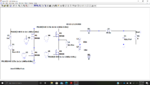
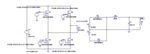
I am designing a full bridge dc-dc converter which is performing a buck operation. Vin=50 Vo=35V, and input power of P=38.28W at a switching frequency of f=150kHz with a current ripple of inductor =0.4 and capacitor voltage ripple = 0.05. L= 26.6uH and C = 416.77nF.

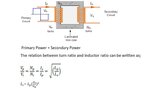
To make the simulation in LT spice I need to know the transformer parameters. Turns ratio of transformer is 2 and Duty of switch is 0.5.

How to obtain the transformer primary inductance Lp and secondary winding inductance Ls and leakage inductance.
I don't know the core specification so please suggest me how to go ahead.
 

Hi,

When I do a simple internet search I find thousands of hits.
What's wrong with them?

Many transformer manufacturers, most SMPS IC manufacturers provide design informations, tools, simulators...
They are for free and made for people who want to design an SMPS ... made for you.

Klaus
 

    Fayaz143

    Points: 2
    Helpful Answer Positive Rating
* When you state buck operation using transformer turns ratio=2 it implies step-down ratio 2:1.

* For a buck converter did you consider doing the classic simpler topology which is made with one inductor and one transistor?

* This simulation compares different inductance values for a transformer primary winding. The output waveforms provide a clue as to the relationship. Notice the wide range of inductance that is efficient enough to be satisfactory (in the area of 1-5 mH). Of course your system requires different component values. In practice, after you obtain the transformer, you can adjust frequency and duty cycle so as to get the desired output.

4 transformer diff pri values 100kHz 240v sq wav load 1200W 30V .png
 
The major problem that I am facing is that I am not able find the formula or equation to find the Lp (primary winding inductance). if I could find the exact formula, them Ls can be easily calculated as Ls= Lp(Ns/Np)^2. Turns ratio is already known. The only unknow parameter is Lp How do we obtain Lp? For any DC-DC isolated transformer (flyback, forward, push-pull and half and full bridge) to carry out the simulation in LT spice we need to know the Lp. Any suggestions or example of how to obtain Lp would help.
 

Attachments

  • Transformer.jpg
    Transformer.jpg
    42.4 KB · Views: 379

Your Ampere throughput calculates to average 1 A per cycle. This means your primary builds to a triangle wave peak of 2A during switch On-time (namely 1/300000 second).

Now you calculate what Henry value achieves this? It's associated with the Inductive time constant formula: L/R
V=50.
R can be 'guesstimated' as any Ohm value that goes with normal operation of a switching converter. Say 1 ohm during switch On-time.

The flux collapses during switch-Off time. To simplify things let's say it drops to zero in 1/300000 second. Is the load resistive or capacitive? 1 Amp goes to the load at 35V, the remaining current goes rapidly to the smoothing capacitor.
 
Thankyou bradtheRad for your suggestions.

My load is a resistive load of 8 Ohms.
To calculate Lp across the transformer primary. On neglecting the resistance of the primary winding and used the standard formula for an inductor
Vin=Lp*di/dt.

I have designed my main inductor with a ripple of 40%. And dt=D/Fs=1/300000 and di=0.4 assuming that di would be same as my main inductor and my Vin=50
Lp=Vin*dt/di=41.25mH and Ls=Lp(N2/N1)^2=10mH
I have simulated my converter ckt. please let me know if my wave form are correct. I am not sure about results and the suggest me the areas where I can improve for better results.
 

Attachments

  • Screenshot (137).png
    Screenshot (137).png
    116.9 KB · Views: 176
  • Screenshot (139).png
    Screenshot (139).png
    35.7 KB · Views: 145
  • Full-Bridge.zip
    1,006 bytes · Views: 120

    lindapcb

    Points: 2
    Helpful Answer Positive Rating
Your schematic is a step-down converter sending bipolar AC through the transformer. However that's not the same as a buck converter.

You give a spec for current ripple (0.4 or 40 percent). This doesn't apply to AC but it normally applies to a single inductor carrying DC. (That's why I mentioned the classic simpler buck converter topology, post #3.) Before going further you need to be certain what topology you wish to design.

Your waveform scale appears to be in milli-Amps. You need current at a level of 1 A or more. To carry that much at 150 kHz, you must reduce the Henry value of your inductor.
 
Thanks BradtheRad for the constant support.

Sorry, the ripple for the main inductor is 0.4.
My project aim is to implement isolated Dc-Dc converter with the transformer. If can not use the ripple of main inductor then how to obtain the ripple (di ) for the primary of the transformer Lp.

I would try your suggestion of lowering the inductance value to bring the current at 1 A level.
 

My project aim is to implement isolated Dc-Dc converter with the transformer. If can not use the ripple of main inductor then how to obtain the ripple (di ) for the primary of the transformer Lp.

Yes isolation requires a transformer. Therefore I think you're seeking to construct a flyback converter. This applies pulsed DC to the primary. A single transistor serves as the switching device.

The secondary side has a diode oriented so that flux collapses as the primary is switched Off. The transformer is operated in a different manner than the everyday method as in your post #6.

Duty cycle 50 percent is commonly the tentative starting point to design for.
And 0.4 current ripple makes sense since the waveform is DC triangle wave.

You ought to be able to locate a schematic at one of the websites which has a calculator for flyback converters.
 
Totally Agree with you BradtheRad.

So I have simulated Flyback converter with Vin=24V and Vo=12 and Io=0.5A with duty ratio =0.5. Load resistance of 24Ohms and C=4.7uF
Lp=120u and Ls=30u with di=1A
I have obtained the desired output using LT spice simulation. Check the wave forms. V(n001)=VLp, which suppose to be voltage across the primary inductor is not exactly a rectangular wave. Why is it not rectangular wave? Are the iLp and iLs current wave forms correct.
 

Attachments

  • Screenshot (148).png
    Screenshot (148).png
    37.6 KB · Views: 128
  • Screenshot (151).png
    Screenshot (151).png
    44.4 KB · Views: 126
  • Screenshot (150).png
    Screenshot (150).png
    29 KB · Views: 133

voltage across the primary inductor is not exactly a rectangular wave. Why is it not rectangular wave? Are the iLp and iLs current wave forms correct.

You made quick progress in the right direction. To smooth the waveforms a few corrections are needed yet.

You have ringing oscillations disturbing one half of the cycle. Usually the cause is LC interaction creating a resonance frequency. Try various capacitor values so that the resonance frequency slows, and so you get smoother output to the load.

Another cause of ringing may be the extra L3 inductor. I believe it's unnecessary in this type of flyback, and you can make it a plain wire.

A snubbing network is normally good design. This is a diode-capacitor-resistor network installed across the primary. It resembles a buck-boost converter. The purpose is to absorb the unavoidable spike when current abruptly stops through an inductor.
The snubber also may reduce the ringing oscillations .
 
you were absolutely right @BradtheRad

L3 inductor was not at all necessary in the circuit.

By increasing the output capacitance value the out voltage and current became more smooth equivalent to Dc without ripples.

I have used snubber circuit as you have suggested and output voltage across the inductor is almost similar to rectangular wave with a small spike.
Are the iL1 and iL2 which are the primary and secondary currents waveforms of the transformer are as expected?

suggest me changes that I should make in Full Bridge converter #6 to get the desired Vo of 35V.
 

Attachments

  • Screenshot (180).png
    Screenshot (180).png
    31.3 KB · Views: 121
  • Screenshot (179).png
    Screenshot (179).png
    44.1 KB · Views: 118

Primary and secondary each appear to carry current during opposite halves of the cycle. Those waveforms appear correct.
I guess the red waveform is correct since the ringing glitch is at the moment of switch-Off, which is normal behavior for inductors.

To step down 50v to 35v, raw math tells you what the turns ratio should be. However if your spec really requires 2:1, then I'm not sure what parameters to adjust.
In any case, by experimenting with various Henry values in both sides of the transformer, you should arrive at your desired performance.

As to current ripple, we could say it's 100 percent right now, since current starts at zero then peaks at an extremely high level during switch-On. To change this, either increase frequency or increase inductor value(s). Eventually you'll be able to reduce current peaks, and thus get by with lower saturation rating.
 
Thanks for your time @BradtheRad

According to my Vin to Vout ratio I took the turns ratio as 1.4 and D=0.5 that exactly satisfy my Inductance of primary and secondary Lp=41.645mH and Ls=21.23mH. I am obtaining undesirable output Vout=1.16V and iout=142mA.

Should I deploy RC snubber in parallel to the mosfets? are my voltage waveform at the terminals of Lp which are V(n007) and V(n008) and primary inductor current iL1 are correct?
 

Attachments

  • Screenshot (191).png
    Screenshot (191).png
    13.7 KB · Views: 138
  • Screenshot (190).png
    Screenshot (190).png
    35.6 KB · Views: 118
  • Screenshot (189).png
    Screenshot (189).png
    37.8 KB · Views: 110

It looks as though you converted to your initial H-bridge plan. Caution because 50V is high voltage hazard for mosfet insulated gates.
To turn on a high-side Nmos, you must apply bias at several volts greater than its source terminal during turn-On. In other words greater than 50V. Consider using Pmos at high side.

For your H-bridge success should come if you play with Henry values in your windings (probably reduce values). It helps if you command several scope traces, and observe how one thing affects another.

This is my simulation of a flyback (with DCR snubber). I adjusted values according to your post #1 specs (more or less). Independently it turned out similar to your post #10 flyback. Mine also displays ringing to an extent.
The snubber resistor needs to dissipate several Watts.

flyback 50v to 30v clkk-driven 150kHz w snub load 40W.png
 
Status
Not open for further replies.

Similar threads

Part and Inventory Search

Welcome to EDABoard.com

Sponsor

Back
Top