kabaleevisu
Advanced Member level 2
- Joined
- Apr 14, 2010
- Messages
- 616
- Helped
- 85
- Reputation
- 170
- Reaction score
- 81
- Trophy points
- 1,308
- Location
- Chennai,India
- Activity points
- 4,512
Hi everyone,
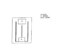
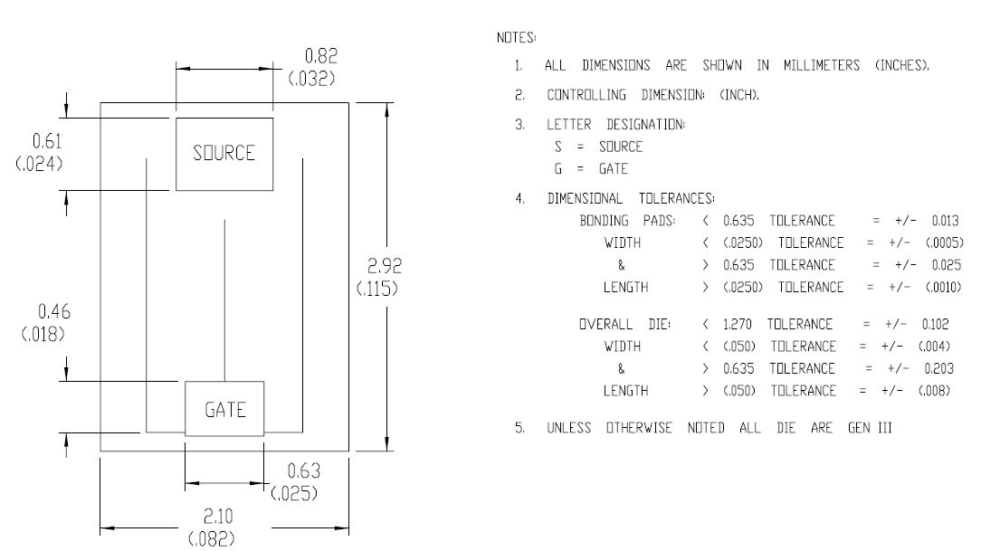
i need to create this Die package.N-channel Power MOSFET has Source ,Gate and Drain pad need to create but in this datasheet ,i have pad size for Gate (widht not mention for Gate) and Source,but Drain mention as Back side.so How to create this Die package.
Package information,

i red some document from that i have some information which i posted below,
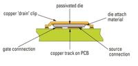