wallacebooth
Newbie level 3
Hi, all:
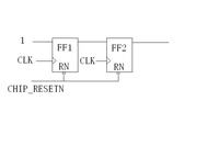
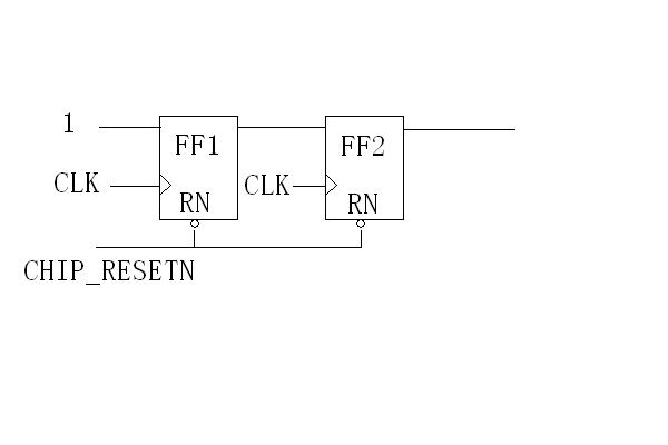
in my design, I use two stage Flip-flop to synchronize asynchronous Reset signal, when synthesis using Synopsys DC, there are Removal violation in FF1 and FF2,
any body who can tell me how can i add constraint to fix these violation?
Thanks a lot!
DC rpt:
Startpoint: CHIP_RESETN
(input port)
Endpoint: osc_sync1_reg
(rising-edge removal check against clock CLK)
Path Group: CLK
Path Type: min
Point Incr Path
--------------------------------------------------------------------------
clock (input port clock) (rise edge) 10.00 10.00
clock network delay (ideal) 0.00 10.00
input external delay 0.00 10.00 r
CHIP_RESETN (in) 0.00 10.00 r
iopad_pad_rstn/C (PISUR) 0.60 10.60 r
pad_rstn (rstc) 0.00 10.60 r
u_OR01/Y (OR2X4) 0.38 10.99 r
osc_sync1_reg/RN (DFFRX1) 0.00 10.99 r
data arrival time 10.99
clock CLK (rise edge) 50.00 50.00
clock network delay (ideal) 0.00 50.00
clock uncertainty 0.10 50.10
osc_sync1_reg/CK (DFFRX1) 0.00 50.10 r
library removal time -0.17 49.93
data required time 49.93
--------------------------------------------------------------------------
data required time 49.93
data arrival time -10.99
--------------------------------------------------------------------------
slack (VIOLATED) -38.94
Startpoint: CHIP_RESETN
(input port)
Endpoint: osc_sync2_reg
(rising-edge removal check against clock CLK)
Path Group: CLK
Path Type: min
Point Incr Path
--------------------------------------------------------------------------
clock (input port clock) (rise edge) 10.00 10.00
clock network delay (ideal) 0.00 10.00
input external delay 0.00 10.00 r
CHIP_RESETN (in) 0.00 10.00 r
iopad_pad_rstn/C (PISUR) 0.60 10.60 r
pad_rstn (rstc) 0.00 10.60 r
u_OR01/Y (OR2X4) 0.38 10.99 r
osc_sync2_reg/RN (DFFRX1) 0.00 10.99 r
data arrival time 10.99
clock CLK (rise edge) 50.00 50.00
clock network delay (ideal) 0.00 50.00
clock uncertainty 0.10 50.10
osc_sync2_reg/CK (DFFRX1) 0.00 50.10 r
library removal time -0.17 49.93
data required time 49.93
--------------------------------------------------------------------------
data required time 49.93
data arrival time -10.99
--------------------------------------------------------------------------
slack (VIOLATED) -38.94