Continue to Site

Welcome to EDAboard.com

Welcome to our site! EDAboard.com is an international Electronics Discussion Forum focused on EDA software, circuits, schematics, books, theory, papers, asic, pld, 8051, DSP, Network, RF, Analog Design, PCB, Service Manuals... and a whole lot more! To participate you need to register. Registration is free. Click here to register now.

how to compensate the opamp w/ a cascode output stage

Status
Not open for further replies.

tommydidi

Member level 1
Joined
Sep 5, 2007
Messages
36
Helped
0
Reputation
0
Reaction score
0
Trophy points
1,286
Activity points
1,494
Hi there,

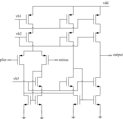
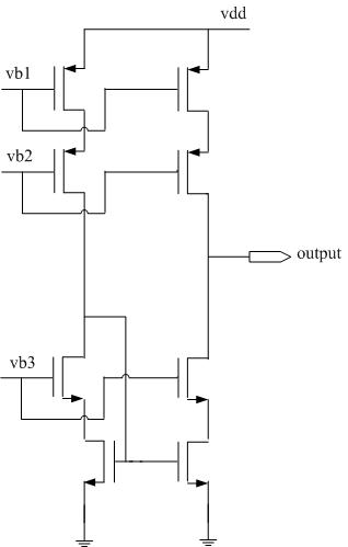
I am designing a two stage opamp (drives a capacitive load) and looking for a way to compensate it. The first stage is a typical pmos input and the second is a cascode one, please see the picture below (only shows the second stage). The "vb1, vb2 and vb3" are bias voltages generated somewhere else in the circuit. I am using the low headroom design for the bottom nmos. I know the cascode opamp is generally self-compensated. After I run the sim, I found the PM is only around 20 degree for some cases. I have played with the cascode pmos and nmos sizes to get the dominant pole moving, it did not help too much though.

I guess I heard a way of compensation by feeding back the output cap, do not know how to do it though. Is it doable? Any other thoughts?

77_1274501727.jpg
 

Hi.

Drains of pmos transistors of input differential pair are connected to the nodes between drains and sources of the upper cascodes, am I right? If yes, this is not two-stage opamp, but one stage opamp. In this case load capacitance performs compensation. If load capacitance doesn't provide desired PM, you can increase load (and PM) by adding a capacitor between output and ground.
 

Hi dedalus,

Thank you for your post. Actually the drain of the pmos input stage IS (not ARE) connected to the nodes between drains and sources of the BOTTOM nmos cascode. The first stage has its own current mirror load. It's two stages for sure.
 

Hi.

Typical approach in the case of two-stage opamp is Miller compensation. It's possible to avoid RHP zero without extra circuitry when cascodes are used. I cannot give answer specific to your amplifier without schematic of the first stage.
 

tommydidi said:
Hi dedalus,

Thank you for your post. Actually the drain of the pmos input stage IS (not ARE) connected to the nodes between drains and sources of the BOTTOM nmos cascode. The first stage has its own current mirror load. It's two stages for sure.

From what you say, it looks like a folded cascode topology. Put in simple words, the output pole of the first stage wouold be at high-frequencies (due to low output impedance of the first stage).

I would advice you to measure the pole pole frequency at the cascode node and at the final output node. As dedalus pointed out, compensating this structure could be attained by increasing the load cap or decreasing the cascode cap.

It would be better if you could post the complete schematic.
 

Thank you guys. Here is the full circuit w/o the bias generator part. I donot want to increase the CLoad cause I have the area constrain. Basically I need a zero at some high frequencies to lift the phase up. So anyway of kicking in a zero?


This is a weird configuration. Putting vb2 transistor in 1st stage is going to cause offset and I don't see any benefit at all. It doesn't increase gain since the other leg doesn't have it.
 

Hi.

This is one stage amplifier! Output of the first stage is connected to the low-impedance node, so it acts as a transconductance stage, not as a voltage amplifier stage: Small-signal output current of the first stage almost entirely flows into the mirror of the second stage. Mirrored current flows through the high output resistance which results in high output voltage: Vout = Vin*Gm[input stage]*R[output stage] => Av = Vout/Vin = Gm[input stage]*R[output stage].

Compensation with load capacitance seems the most effective for this circuit.

tommydidi said:
Basically I need a zero at some high frequencies to lift the phase up. So anyway of kicking in a zero?

You can try Miller compensation technique. Series capacitor and resistor (transistor) between input and output nodes of the output stage will introduce zero. Theoretically it's possible to cancel second pole with this zero. But as far as I know this technique is not used, because it's hard to track poles' position across PVT variations.

love_analog said:
Putting vb2 transistor in 1st stage is going to cause offset and I don't see any benefit at all.

This transistor (I suppose you've meant vb3 transistor) is used to agree DC output of the input stage with DC input of the output stage. Wide-swing cascode current mirror have to be replaced with standard cascode without it.
 

Status
Not open for further replies.

Similar threads

Part and Inventory Search

Welcome to EDABoard.com

Sponsor

Back
Top