Continue to Site

Welcome to EDAboard.com

Welcome to our site! EDAboard.com is an international Electronics Discussion Forum focused on EDA software, circuits, schematics, books, theory, papers, asic, pld, 8051, DSP, Network, RF, Analog Design, PCB, Service Manuals... and a whole lot more! To participate you need to register. Registration is free. Click here to register now.

How to compare multiple voltages ( II )

Status
Not open for further replies.

timedate

Member level 5
Joined
Jun 20, 2010
Messages
81
Helped
0
Reputation
0
Reaction score
0
Trophy points
1,286
Location
germany
Activity points
1,952
I try to simplify my questions in the last thread , then I realized I failed...

Here is my original question....

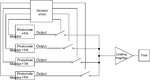
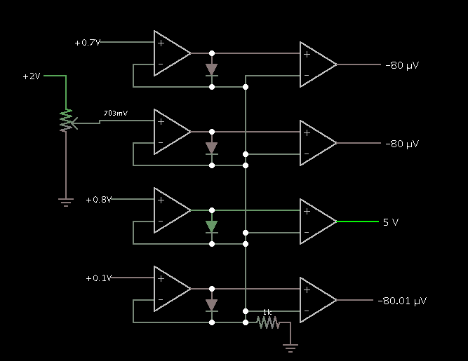
I try to build a photodiode array which contains 4 photodiodes. Each photodiode is connected with its own TIA (transimpedance amplifier), and then connected to LA (Limiting amplifier) through a switch.

I want choose the photodiode which receives largest optical power, turn on the switch, connected with LA. Meanwhile, turn off the other 3 switches.

The TIA I am using has the function that can monitor the current flow through the TIA (pin 'monitor'). So, by comparing this current (actually, it is the voltage) I can know which photodiode tcan receive the largest optical power.

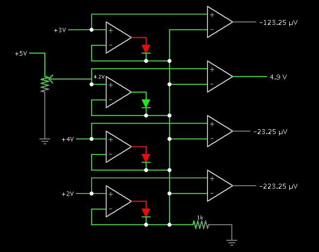
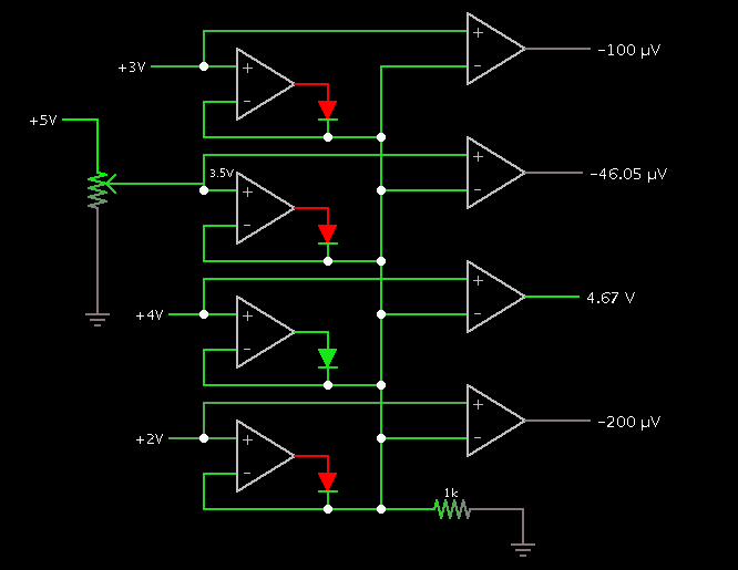
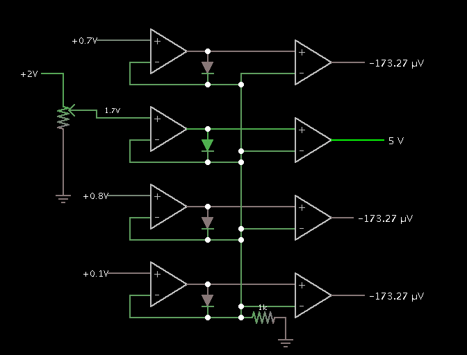
Attached is my schematic, the question is , which is simplest way to achieve the "decision circuit"? could this pure analog? avoid using FPGA? for example using 3 comparators....

*
 

Attachments

  • maxim.jpg
    maxim.jpg
    253.9 KB · Views: 153

Start with 6 comparators. Each has 2 inputs.

These examine all combinations of 2 detectors.
#1 compares signals from detector 1 & 2.
#2 compares signals from detector 1 & 3.
#3 compares signals from detector 1 & 4.
#4 compares signals from detector 2 & 3.
#5 compares signals from detector 2 & 4.
#6 compares signals from detector 3 & 4.

The outputs are either high or low.

A particular series of 1's and 0's will emerge, depending on which of the four detectors tops the other three.

Route it through an array of steering diodes (or a network of logic gates), to a one-of-four selector.
Right off the bat I can't visualize just what such a network would look like, but it seems like it ought to be possible.

- - - Updated - - -

If comparators 3,5,6 are all high, this means detector #4 tops the others. Switch to channel 4.

If comparators 2 & 4 are high, and 6 is low, then switch to channel 3.

If comparator 1 is high, and 4,5 are low, then switch to channel 2.

If comparators 1,2,3 are low, then switch to channel 1.

On second thought, it takes extra devices to test for some high, some low.

Better to start with 12 comparators, and test each detector against the other 3. Then examine for 3 high values from the pertinent comparators, using a 3-input AND gate. You'll need four 3-input AND gates.
 
Last edited:
I just thought of a simple "winner-takes-all network" as, for example, the paper by Donckers. Simple, small and elegant. I used a similar configuration to compare 320 current years ago.
 
The intended decision criterion isn't clearly specified, I think.

We can either imagine it as a kind of max() function for the instantaneous TIA output levels, or a delayed decision e.g. based on average values. In the latter case, an exact definition would be needed.
 

I just thought of a simple "winner-takes-all network" as, for example, the paper by Donckers. Simple, small and elegant. I used a similar configuration to compare 320 current years ago.

Well, this "winner take all" seems good for me. Do you know is there any Commercial “WTA” IC to buy ?

- - - Updated - - -

The intended decision criterion isn't clearly specified, I think.

We can either imagine it as a kind of max() function for the instantaneous TIA output levels, or a delayed decision e.g. based on average values. In the latter case, an exact definition would be needed.

The former case. Once the comparison of the input changes, output changes instantaneous. (by the way, the input doesn't change so often)

- - - Updated - - -

On second thought, it takes extra devices to test for some high, some low.

Better to start with 12 comparators, and test each detector against the other 3. Then examine for 3 high values from the pertinent comparators, using a 3-input AND gate. You'll need four 3-input AND gates.


Such a Genius idea, if i can not buy any "WTA" circuit, I think I will start with comparators...
 

You can use four of these precision rectifiers with the diode outputs tied together as I suggested in your previous thread. Then you add a comparator directly at each op amp output to detect which output is >0V since only the op amp with the highest input will have a positive output. The comparator output controls its respective switch. You can do that with one quad op-amp such as the LM324, four diodes, and one quad comparator such as the LM339.
 
Last edited:

You can use four of these precision rectifiers with the diode outputs tied together as I suggested in your previous thread. Then you add a comparator directly at each op amp output to detect which output is >0V since only the op amp with the highest input will have a positive output. The comparator output controls its respective switch. You can do that with one quad op-amp such as the LM358, four diodes, and one quad comparator such as the LM339.

Your method works. The green diode marks the highest signal in the simulations below.

The left diagram has signal 2 highest. (Observe volt level on incoming wire from the pot.)
The right diagram has signal 3 highest.


Power supply is assumed to be 5V.

There seems to be an unusual case when all signals are less than 0.6 V. Then the right-hand output may be less than supply V.

- - - Updated - - -

Update to the above:

Here is a revised layout which works better since it fits Crutschow's description better.
The winning right-hand output is never less than supply V.


BradtheRad, your last circuit is a slight variation on the design I had in mind, which connects the comparator output minus input to ground rather than the combined output, but either way works.

Edit: On second thought, your approach is slightly better since mine may have a problem due to amplifier offset voltage in single supply applications. This could mean a comparator wouldn't go low when the "off" op amp output is near 0V. This would require adding a small positive offset voltage (adding a couple more resistors) to the comparator plus inputs. With your design, there is not a problem with that.
 
Last edited:

Well, this "winner take all" seems good for me. Do you know is there any Commercial “WTA” IC to buy ?
I am not aware of off the shelf WTA ICs. I thought you where designing the IC.
 

BradtheRad, your last circuit is a slight variation on the design I had in mind, which connects the comparator output minus input to ground rather than the combined output, but either way works.

Edit: On second thought, your approach is slightly better since mine may have a problem due to amplifier offset voltage in single supply applications. This could mean a comparator wouldn't go low when the "off" op amp output is near 0V. This would require adding a small positive offset voltage (adding a couple more resistors) to the comparator plus inputs. With your design, there is not a problem with that.

Just the same you get the award for elegance and lower parts count.

I knew I had to find out whether your method would work, seeing how it prospectively would be more efficient than the best I could think up (post #2).

My method would use 3 quad comparator IC's, and a couple of triple 3-input AND gate IC's (or the equivalent).
 

Hi, @BradtheRad and @crutschow thanks all. I make my decision to build the circuit like your suggestions, all thought in the LTspice simulation, I still get some problems during the input signal transition time.


Just the same you get the award for elegance and lower parts count.

I knew I had to find out whether your method would work, seeing how it prospectively would be more efficient than the best I could think up (post #2).

My method would use 3 quad comparator IC's, and a couple of triple 3-input AND gate IC's (or the equivalent).


BradtheRad, your last circuit is a slight variation on the design I had in mind, which connects the comparator output minus input to ground rather than the combined output, but either way works.

Edit: On second thought, your approach is slightly better since mine may have a problem due to amplifier offset voltage in single supply applications. This could mean a comparator wouldn't go low when the "off" op amp output is near 0V. This would require adding a small positive offset voltage (adding a couple more resistors) to the comparator plus inputs. With your design, there is not a problem with that.
 

Hi, @BradtheRad and @crutschow thanks all. I make my decision to build the circuit like your suggestions, all thought in the LTspice simulation, I still get some problems during the input signal transition time.
What type of problems?

Post the LTspice .asc file of your simulation.
 

HI, @crutschow

Attached is my four simulations, the ideal1 and ideal2 use ideal opamps in LTspice, while the real3 and real4 use the real LT1001 opamp.

in ideal1 and real3, i compare the in- with in+ , like the first version of BradtheRad's circuit.
in ideal2 and real4. i compare the in- with the opamp output node , like the modified version of BradtheRad's circuit.

The problem is:

1 for the ideal opamp, it doesn't work, during the transition time...

2 for the real opamp, see real_multiple comparator 3, I get two problems

a: First and the most important, when I see the out1 and out2, there is a short time both out1 and out2 are low (around 0.4ms), while I want at least one output remains high...

b: for the 3rd opamp, its input signal is 0.7v, which is always smaller than the first one (0.8v), that means the output3 should always be low. However, in the simulation, there exist a short pulse.
Of course, this short pulse will disappear when is input signal is further decreased to 0.5v.


What type of problems?

Post the LTspice .asc file of your simulation.
 

Attachments

  • Spice.zip
    4 KB · Views: 98

The circuit you want to use is #4. I didn't look at the ideal circuit ones since ideal circuit models can sometimes give strange results.

#3 will not work properly as you have seen since, for the comparator at the trip point, the two input voltages to the comparator are essentially equal. Why are you concerned about that circuit? BradtheRad said he had a problem with it also.

#4 appears to work correctly. Do you have a problem with that one? There may be a crossover point when two comparators in transition are either momentarily both high or low but that is unavoidable due to the finite response time of real circuits.

You can eliminate a negative supply if you use a single-supply type op amp.
 

Well, Thanks a lot, I will build a PCB for #4


The circuit you want to use is #4. I didn't look at the ideal circuit ones since ideal circuit models can sometimes give strange results.

#3 will not work properly as you have seen since, for the comparator at the trip point, the two input voltages to the comparator are essentially equal. Why are you concerned about that circuit? BradtheRad said he had a problem with it also.

#4 appears to work correctly. Do you have a problem with that one? There may be a crossover point when two comparators in transition are either momentarily both high or low but that is unavoidable due to the finite response time of real circuits.

You can eliminate a negative supply if you use a single-supply type op amp.
 

There is one concern to be aware of when building the circuit. The op amp outputs that are inactive go to the negative rail which may exceed the negative voltage input rating of the comparator if you are using a dual supply for the op amps. Thus you either need to use a single supply op amp powered from a plus voltage and ground, or add a resistor and Schottky diode clamp between each op amp output and its respective minus input.
 

well, why using the dual supply will cause this problem...?

My simulation shows that, dual supply is OK, and single supply doesn't work.

Attached is my signal supply circuit. it may need 5 mins to run the simulation.


There is one concern to be aware of when building the circuit. The op amp outputs that are inactive go to the negative rail which may exceed the negative voltage input rating of the comparator if you are using a dual supply for the op amps. Thus you either need to use a single supply op amp powered from a plus voltage and ground, or add a resistor and Schottky diode clamp between each op amp output and its respective minus input.


update:

actually, I also find some opamps works in the signal supply, for example LT1079, I thinks it may depends on the opamp, although I don't know depends on which specification (offset bandwidth...)
 

Attachments

  • single supply.zip
    1 KB · Views: 90
Last edited:

Status
Not open for further replies.

Similar threads

Part and Inventory Search

Welcome to EDABoard.com

Sponsor

Back
Top