SIDDHARTHA HAZRA
Advanced Member level 4
Hi subbu2 ,
PLEASE ASK YOUR QUESTION IN A SEPARATE POST ...
- - - Updated - - -
Hi anhnha,
Good to see that you have designed an error amplifier as suggested by others ...
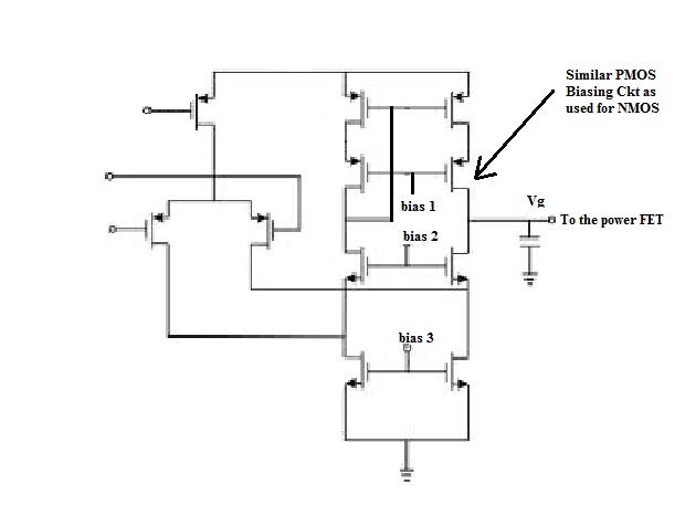
A few things to note: Keeping a few MOSFETs into sub-threshold in fact helpful. As you know that a MOSFET contributes more gm if it is in sub-threshold. If you know which all MOSFETs are contributing gm in your gain equation then you can get higher gain by making those MOSFETs operate in sub-threshold. You can keep M3&M4 and M11&M12 in sub-threshold as the gain equation is Av = gm3 * (ro13 || gm12*r012*ro8) (approx ) (In your ckt)
Again the MOSFETs in the bias arm M2 and M5 should be also be in sub-threshold for proper bias generation for M11 & M12
Let us know your observations ..... Hope this will help ..")
Evn I am designing an LDO with following specs..
Vin : 1.8V +/- 10%
Vout : 1.5V +/- 3%
Vref : 1V +/- 1%
Iload : 0 to 50mA
Ext Cap : 100nF +/- 20%
PSR : >40dB upto 10MHz
Can anybody please explain me which method is better whether to proceed block by block like designing error amp then moving on to power mosfet etc...or whether to simulate the whole LDO circuit and then analyse..
please suggest me the way forward..I have read abt the Single stage diff amp and abt miller compensation after adding second stage and yet to start wit the design.
PLEASE ASK YOUR QUESTION IN A SEPARATE POST ...
- - - Updated - - -
Hi anhnha,
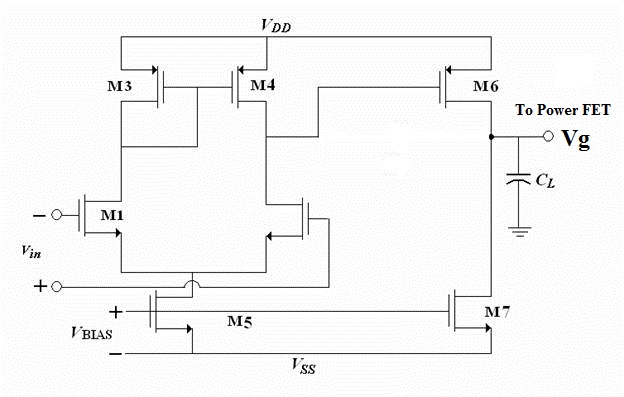
I chose Vbias1, Vbias2, and Vbias3 all above the threshold voltage of NMOS transistors a little and therefore, M5, M8, M9, M10, and M11 all are in saturation. However, the problem here is that all the rest transistors are NOT in saturation.
M3: Saturation GOOD
M4: Linear: WRONG.
M1: Subthreshold: WRONG
M2: Subthreshold: WRONG.
M6: Saturation: GOOD
M7: Saturation: GOOD
M8: Subthreshold: WRONG.
M9: Subthreshold: WRONG.
Mp: Saturation: GOOD
Good to see that you have designed an error amplifier as suggested by others ...
A few things to note: Keeping a few MOSFETs into sub-threshold in fact helpful. As you know that a MOSFET contributes more gm if it is in sub-threshold. If you know which all MOSFETs are contributing gm in your gain equation then you can get higher gain by making those MOSFETs operate in sub-threshold. You can keep M3&M4 and M11&M12 in sub-threshold as the gain equation is Av = gm3 * (ro13 || gm12*r012*ro8) (approx ) (In your ckt)
Again the MOSFETs in the bias arm M2 and M5 should be also be in sub-threshold for proper bias generation for M11 & M12
Let us know your observations ..... Hope this will help ..