mohamis288
Full Member level 3
Hello,
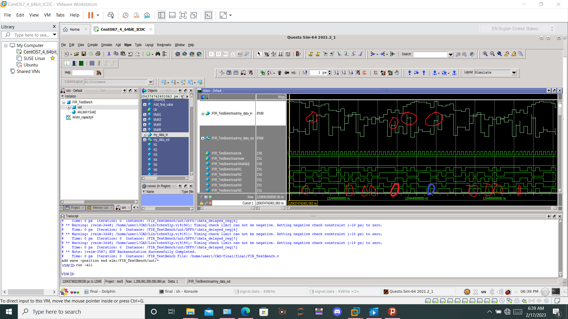
My design (8-bit FIR filter) in Questa acts unexpectedly. this occurs at the clock edge. for example in the following image, you can see, some internodes have a jump. in the following image, I have shown some of the jumps in the internodes and output analog signal.

as shown in the log file, a warning is:
negative check constrant WARNINGS are related to outputs of flip-flops. is this causing any problem?
also some of the warnings are related to the connections. When I synthesized My Verilog code in the 'Design vision', I checked schematic view. nothing was floated.
Also when I was synthesizing my project in 'Design vision', the following warning was shown:
can you tell me how can I resolve this? this is my first project with VLSI design.
BR
My design (8-bit FIR filter) in Questa acts unexpectedly. this occurs at the clock edge. for example in the following image, you can see, some internodes have a jump. in the following image, I have shown some of the jumps in the internodes and output analog signal.
as shown in the log file, a warning is:
Code:
#

# Compile of FIR_TestBench.v was successful.
# Compile of netlist.v was successful.
# Compile of tcbn65lp.v was successful.
# 3 compiles, 0 failed with no errors.
vsim -sdftyp /uut=/home/user1/CAD/final/netlist9.sdf work.FIR_TestBench
# End time: 18:10:00 on Feb 17,2023, Elapsed time: 0:05:05
# Errors: 0, Warnings: 109
# vsim -sdftyp "/uut=/home/user1/CAD/final/netlist9.sdf" work.FIR_TestBench
# Start time: 18:10:00 on Feb 17,2023
# ** Note: (vsim-3813) Design is being optimized due to module recompilation...
# Loading work.FIR_TestBench(fast)
# Loading work.FIR_Filter(fast)
# Loading work.DFCNQD1(fast)
# Loading work.CKND0(fast)
# Loading work.FA1D0(fast)
...
...
...

# Loading work.NR2D0(fast)
# Loading work.AN2D0(fast)
# Loading work.MAOI22D0(fast)
# Loading instances from /home/user1/CAD/final/netlist9.sdf
# Loading timing data from /home/user1/CAD/final/netlist9.sdf
# ** Warning: (vsim-SDF-16107) /home/user1/CAD/final/netlist9.sdf(193): The interconnect '/FIR_TestBench/uut/my_data_in' is not connected to the destination '/FIR_TestBench/uut/U38/A2'.
# The interconnect request will be replaced with a port annotation at the destination.
# ** Warning: (vsim-SDF-16107) /home/user1/CAD/final/netlist9.sdf(195): The interconnect '/FIR_TestBench/uut/my_data_in' is not connected to the destination '/FIR_TestBench/uut/U37/A2'.
# The interconnect request will be replaced with a port annotation at the destination.
# ** Warning: (vsim-SDF-16107) /home/user1/CAD/final/netlist9.sdf(197): The interconnect '/FIR_TestBench/uut/my_data_in' is not connected to the destination '/FIR_TestBench/uut/U36/A2'.
# The interconnect request will be replaced with a port annotation at the destination.
# ** Warning: (vsim-SDF-16107) /home/user1/CAD/final/netlist9.sdf(205): The interconnect '/FIR_TestBench/uut/my_data_in' is not connected to the destination '/FIR_TestBench/uut/U31/A1'.
# The interconnect request will be replaced with a port annotation at the destination.
# ** Warning: (vsim-SDF-16107) /home/user1/CAD/final/netlist9.sdf(209): The interconnect '/FIR_TestBench/uut/my_data_in' is not connected to the destination '/FIR_TestBench/uut/U30/C'.
# The interconnect request will be replaced with a port annotation at the destination.
# ** Warning: (vsim-SDF-16107) /home/user1/CAD/final/netlist9.sdf(266): The interconnect '/FIR_TestBench/uut/my_data_in' is not connected to the destination '/FIR_TestBench/uut/add_2_root_add_51_6/U2/A1'.
# The interconnect request will be replaced with a port annotation at the destination.
# ** Warning: (vsim-SDF-16107) /home/user1/CAD/final/netlist9.sdf(268): The interconnect '/FIR_TestBench/uut/my_data_in' is not connected to the destination '/FIR_TestBench/uut/add_2_root_add_51_6/U1/A1'.
# The interconnect request will be replaced with a port annotation at the destination.
# ** Warning: (vsim-SDF-16107) /home/user1/CAD/final/netlist9.sdf(286): The interconnect '/FIR_TestBench/uut/my_data_in' is not connected to the destination '/FIR_TestBench/uut/add_2_root_add_51_6/U1_2/B'.
# The interconnect request will be replaced with a port annotation at the destination.
# ** Warning: (vsim-SDF-16107) /home/user1/CAD/final/netlist9.sdf(414): The interconnect '/FIR_TestBench/uut/my_data_in' is not connected to the destination '/FIR_TestBench/uut/DFF0/\data_delayed_reg[0] /D'.
# The interconnect request will be replaced with a port annotation at the destination.
# ** Warning: (vsim-SDF-16107) /home/user1/CAD/final/netlist9.sdf(417): The interconnect '/FIR_TestBench/uut/my_data_in' is not connected to the destination '/FIR_TestBench/uut/DFF0/\data_delayed_reg[1] /D'.
# The interconnect request will be replaced with a port annotation at the destination.
# ** Warning: (vsim-3448) /home/user1/CAD/Lib/tcbn65lp.v(9191): Timing check limit can not be negative. Setting negative check constraint (-10 ps) to zero.
#    Time: 0 ps  Iteration: 0  Instance: /FIR_TestBench/uut/DFF5/\data_delayed_reg[0]
# ** Warning: (vsim-3448) /home/user1/CAD/Lib/tcbn65lp.v(9190): Timing check limit can not be negative. Setting negative check constraint (-10 ps) to zero.
#    Time: 0 ps  Iteration: 0  Instance: /FIR_TestBench/uut/DFF5/\data_delayed_reg[0]
# ** Warning: (vsim-3448) /home/user1/CAD/Lib/tcbn65lp.v(9191): Timing check limit can not be negative. Setting negative check constraint (-10 ps) to zero.
#    Time: 0 ps  Iteration: 0  Instance: /FIR_TestBench/uut/DFF5/\data_delayed_reg[1]
...
...
...
...

# ** Note: (vsim-3587) SDF Backannotation Successfully Completed.
#    Time: 0 ps  Iteration: 0  Instance: /FIR_TestBench File: /home/user1/CAD/final/final/FIR_TestBench.v
add wave -position end sim:/FIR_TestBench/uut/*
run -all
negative check constrant WARNINGS are related to outputs of flip-flops. is this causing any problem?
also some of the warnings are related to the connections. When I synthesized My Verilog code in the 'Design vision', I checked schematic view. nothing was floated.
Also when I was synthesizing my project in 'Design vision', the following warning was shown:
Code:
verilog 'assign' or 'tran' statements are written out. (vo-4)can you tell me how can I resolve this? this is my first project with VLSI design.
BR
Last edited: