bellona
Junior Member level 2
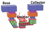
I'm layouting an LNA with SiGe BiCMOS process. Since the Emitter resistance degenerates the gain, I'd like to double connect the NPN's emitter, as shown in this picture:

The problem is: How can I assign different terminal for the two ends of the Emitter metal (marked with red arrow)? Normally I could only assign one terminal for this Emitter metal, which would defeat my purpose of simulating the parasitic resistance effect on the circuit's gain. Same thing happens to double contacted Base to lower the Noise Factor.
I'v did some search in this Board, and I've found one post that suggests the use of LVS BOX.
https://www.edaboard.com/threads/244987/
Are there any alternative ways to do this? Thx
- - - Updated - - -
I found that the PDK I'm using actually supports this function through a device called lvsres. It creates an artifical metal resistor for LVS purpose. All I need to do is to mark the path with associated 'Mx' 'res' layer on top of the 'Mx' 'DG' layer.