luciforlove
Member level 1

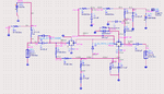
here is the schematic.
2 at41485 as amplifier
at41485 1dB point is 18dBm when ic=40mA
on this schematic's instruction,it is said the LNA's 1dBpoint is 7dBm
but when i test it with Network Analyzer
S21 is 28dB when input is -20dBm,thats right
but when input is -10dbm s21=-20dB
when input is 0dbm,the gain is as low as 9
i really which part of this schem make this happen?how it works?and why design like that?
ps :Attached Thumbnails is not right ,idont know how to delete it
Attachments
Last edited:
 utput power, 1dB compression is 7dBm >