Continue to Site

Welcome to EDAboard.com

Welcome to our site! EDAboard.com is an international Electronics Discussion Forum focused on EDA software, circuits, schematics, books, theory, papers, asic, pld, 8051, DSP, Network, RF, Analog Design, PCB, Service Manuals... and a whole lot more! To participate you need to register. Registration is free. Click here to register now.

How is the block design utilizing a specific IP core supposed to be designed when using the IP C code examples in Vitis?

Status
Not open for further replies.

arminb73

Junior Member level 3
Joined
Nov 9, 2021
Messages
26
Helped
0
Reputation
0
Reaction score
1
Trophy points
3
Activity points
185
When wanting to experiment with different IPs as an example the AXI UART16550 how is one supposed to design the block design in order to make the Xilinx C examples "correspond" well with the exported block design.

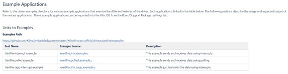
As an example. When wanting to experiment with this C code:
https://github.com/Xilinx/embeddeds.../uartns550/examples/xuartns550_intr_example.c

How am I supposed to do the block design connection in Vivado before exporting the hardware to be used in Vitis?
 

Well I did not completely understand your question.

If you want some software to control your hardware IPs then your software(C code) should run on a microprocessor. It can be a ARM hard macro, or Microblaze or RISCV core and needs to be present within your hardware design. Up to this point, the hardware architecture is this CPU, UART IP, clocks and resets (I will not go in to the details here). After you have such a hardware design ready, you need to export the hardware so that using Xilinx SDK you can write the C code that will run on the targeted CPU.

I see that the .c you have posted above uses interrupts. You need to understand how to design it in hardware and how it is used by the software.
 
Last edited:

Well I did not completely understand your question.

If you want some software to control your hardware IPs then your software(C code) should run on a microprocessor. It can be a ARM hard macro, or Microblaze or RISCV core and needs to be present within your hardware design. Up to this point, the hardware architecture is this CPU, UART IP, clocks and resets (I will not go in to the details here). After you have such a hardware design ready, you need to export the hardware so that using Xilinx SDK you can write the C code that will run on the targeted CPU.
Your point is well taken. The program does, in fact, need the use of four different IP addresses:

* CPU
* UART
* CLOCKS
* INTERCONNECT
* RESET

What I'm not sure about is how they're meant to be linked together. To ensure that the software code and the hardware design are in sync.

Regards,
Armin
 

What I'm not sure about is how they're meant to be linked together. To ensure that the software code and the hardware design are in sync.
By "linked together" should I understand hardware connection?
If yes, then take a look at any Xilinx based "Hello World" design using AXI UART16550. All those IPs will be used and connected in such a design.
 

By "linked together" should I understand hardware connection?
If yes, then take a look at any Xilinx based "Hello World" design using AXI UART16550. All those IPs will be used and connected in such a design.
Yes, indeed hardware connection. Where can I find these designs? Would really appreciate having that as a reference point.
 

Hi,

maybe there is a misunderstanding about "IP".
IP- core means "Intellectual Property" (post #1)
IP- address means "Internet Prococol" (post #3)

These completely are different things.
An IP core does not need an IP address.

Klaus
 

Hi,

maybe there is a misunderstanding about "IP".
IP- core means "Intellectual Property" (post #1)
IP- address means "Internet Prococol" (post #3)

These completely are different things.
An IP core does not need an IP address.

Klaus
Sorry, I was too quick on the keyboard. I am discussing the intellectual properties.
 

Your point is well taken. The program does, in fact, need the use of four different IP addresses:

* CPU
* UART
* CLOCKS
* INTERCONNECT
* RESET

What I'm not sure about is how they're meant to be linked together. To ensure that the software code and the hardware design are in sync.

Regards,
Armin
Hello @arminb73,

the key idea behind such block designs is AXI Bus - Memory-Mapped (with address lines) or Stream(only data - not address lines). Then in HARD-CPU (ARM) there are two parts PS and PL and these parts are comunicating each othert by AXI Busses. On each Block-design is "Adresses Editor" in which you have to map your intefaces into CPU space adresses. Then writting programs in C is writing and reading registers alocated by these adresses. It is difficult and one have to have big experience with doing this.
In this post on polish forum I gave many links to series of lectures related to the topics about you are asking:

https://forbot.pl/forum/topic/20717...-w-xilinx-vivado/?tab=comments#comment-173812

You can translate this WWW page to English with "goole Translate" in easy way.

Best regards


If I understand you correctly, you are looking for a so called "Vitis Platform Creation" - hardware created in Vivado and then exported to Vitis (a successor of Xilinx SDK).

Vivado example design:

All you need to do is to run in Vivado the following command in the TCL Console:
source system_step1.tcl
Then the whole project will be generated (with an address map) ready to be exported to use in Vitis.

Reference:

You can search for repos/projects with an IP core of your interest - AXI UART16550.
Often only .tcl files are available in repos.
 
Last edited:

Consider the following scenario: I want to run these sample applications. Given that these examples are aimed at the UART-lite, I know that the Vivado block design will include the AXI Uartlite IP. Also, because I am working with multiple applications, it is natural for me to assume that the block design must include the Processing system.

What I'm not sure about is how the connections between the IPs are supposed to be made so that the applications make sense.

Please if someone could give me any advice I would highly appreciate it.

The examples are found at the following website:
 

Attachments

  • examples_uart_lite.jpg
    examples_uart_lite.jpg
    125.9 KB · Views: 117

What you have posted above is the software which runs on a uProcessor that can control the design. But first you must create the hardware design itself before you proceed to write the software for it.

What I'm not sure about is how the connections between the IPs are supposed to be made so that the applications make sense.
If you do not know how to connect clocks, resets and bus in a digital design, then I am afraid you are having a very fundamental problem. Someone has posted vdo tutorials above, have you followed them?
To teach basic things such as port connections is in my opinion out of scope for this forum!
 

What you have posted above is the software which runs on a uProcessor that can control the design. But first you must create the hardware design itself before you proceed to write the software for it.


If you do not know how to connect clocks, resets and bus in a digital design, then I am afraid you are having a very fundamental problem. Someone has posted vdo tutorials above, have you followed them?
To teach basic things such as port connections is in my opinion out of scope for this forum!
The issue is not connecting the IPs to one another. The issue is how the different IPs are supposed to be connected when the example software design is taken into account.
 

The issue is how the different IPs are supposed to be connected when the example software design is taken into account.
This is hardware design! You must think about the hardware architecture first, design the hardware itself as the 2nd step and then comes the software part. The reverse sequence will not work.
 

Status
Not open for further replies.

Part and Inventory Search

Welcome to EDABoard.com

Sponsor

Back
Top