neazoi
Advanced Member level 6
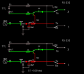
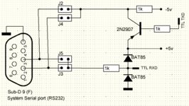
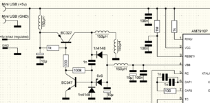
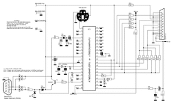
How does this UART to RS-232 converter work?
I see a negative charge pump, which is driven by an oscillator (200khz square wave, internal to the chip).
Then the PNP switches between a negative voltage of the pump and the positive (depended on the data on it's base pin), for the differential requirements of the RS-232 (compatible). But how does it do this switching, I am confused.
Attachments
Last edited: