Continue to Site

Welcome to EDAboard.com

Welcome to our site! EDAboard.com is an international Electronics Discussion Forum focused on EDA software, circuits, schematics, books, theory, papers, asic, pld, 8051, DSP, Network, RF, Analog Design, PCB, Service Manuals... and a whole lot more! To participate you need to register. Registration is free. Click here to register now.

How do I set a good static work point to a fully differential telescope OPAMP?

Status
Not open for further replies.

yeknight

Newbie level 4
Joined
Mar 13, 2011
Messages
7
Helped
0
Reputation
0
Reaction score
0
Trophy points
1,281
Activity points
1,359
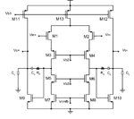
I am designing a fully differential telescope OPAMP,but can not let all the mosfets work in Saturati,How do I set a good static work point to a fully differential telescope OPAMP?
 

yeknight,

Show your schematic please,
That Vth of mosfets and supply voltage of OPAMP?

Best reguards
 
Apparently with your design choises,you have violated the saturation constraint Vds>Vdsat.
Show a schematic with the Vdsat of each transistor along with the DC Operating Point after DC simulation.
 

111.png
.Title Operational Amplifier
.lib "C:\hspice\CMOS_035_Spice_Model.lib" TT

.option list post node

.PARAM W2=12U
.PARAM W1=20U
.PARAM W3=12U
.PARAM W4=20U

**************OTA with 2nd stage*************************
M1 1 in1 3 vdd p_33 W = W1 L = 1u
M2 4 in2 3 vdd p_33 W = W1 L = 1u
M3 5 vb1 1 vdd p_33 W = W4 L = 1u
M4 7 vb1 4 vdd p_33 W = W4 L = 1u
M5 5 vb2 10 vss n_33 W = W3 L = 1u
M6 7 vb2 11 vss n_33 W = W3 L = 1u
M7 10 vb3 vss vss n_33 W = W2 L = 1u
M8 11 vb3 vss vss n_33 W = W2 L = 1u
M13 3 13 vdd vdd p_33 W = 50u L = 1u
M11 14 13 vdd vdd p_33 W = 150u L = 1u
M12 15 13 vdd vdd p_33 W = 150u L = 1u
M9 14 5 vss vss n_33 W = 60u L = 1u
M10 15 7 vss vss n_33 W = 60u L = 1u

R1 5 16 1K
C1 16 14 1p
R2 17 7 1K
C2 17 15 1p
C3 14 vss 3p
C4 15 vss 3p

Vdd vdd 0 3.5V
Vss vss 0 0V


VB1 vb1 0 0.89V
VB2 vb2 0 1.57V
VB3 vb3 0 0.97V
VB4 13 0 2.27V


.op
Vin1 in1 0 dc 1.5 ac 1 0
Vin2 in2 0 dc 1.5 ac 1 180
.ac dec 100 1 1e4
.END


**** mosfets


subckt
element 0:m1 0:m2 0:m3 0:m4 0:m5 0:m6
model 0:p_33 0:p_33 0:p_33 0:p_33 0:n_33 0:n_33
region Linear Linear Linear Linear Saturati Saturati
id -96.8843u -96.8843u -96.8843u -96.8843u 96.8843u 96.8843u
ibs 8.5987f 8.5987f 12.4608f 12.4608f -378.8958a -378.8958a
ibd 12.4679f 12.4679f 15.1091f 15.1091f -2.4996f -2.4996f
vgs -1.7390 -1.7390 -2.2317 -2.2317 1.1090 1.1090
vds -117.2495m -117.2495m -80.3166m -80.3166m 2.5804 2.5804
vbs 261.0376m 261.0376m 378.2872m 378.2872m -461.0063m -461.0063m
vth -882.1395m -882.1395m -901.0780m -901.0780m 809.5577m 809.5577m
vdsat -777.7688m -777.7688m -1.1833 -1.1833 282.9059m 282.9059m
beta 1.1381m 1.1381m 1.0307m 1.0307m 2.0534m 2.0534m
gam eff 350.8938m 350.8938m 351.0603m 351.0603m 704.1687m 704.1687m
gm 102.9562u 102.9562u 54.2859u 54.2859u 562.8844u 562.8844u
gds 760.1425u 760.1425u 1.1659m 1.1659m 1.3475u 1.3475u
gmb 22.2185u 22.2185u 13.8119u 13.8119u 168.1881u 168.1881u
cdtot 138.2412f 138.2412f 143.4489f 143.4489f 12.1728f 12.1728f
cgtot 111.7974f 111.7974f 112.2072f 112.2072f 49.6537f 49.6537f
cstot 136.2200f 136.2200f 135.7319f 135.7319f 68.2172f 68.2172f
cbtot 93.0827f 93.0827f 89.7160f 89.7160f 43.2142f 43.2142f
cgs 60.8942f 60.8942f 58.0692f 58.0692f 42.6498f 42.6498f
cgd 49.4182f 49.4182f 52.7260f 52.7260f 1.7577f 1.7577f


subckt
element 0:m7 0:m8 0:m13 0:m11 0:m12 0:m9
model 0:n_33 0:n_33 0:p_33 0:p_33 0:p_33 0:n_33
region Saturati Saturati Linear Saturati Saturati Linear
id 96.8843u 96.8843u -193.7686u -868.8520u -868.8520u 868.8521u
ibs -1.702e-20 -1.702e-20 4.782e-19 2.0956a 2.0956a -1.373e-19
ibd -378.8618a -378.8618a 20.5767f 118.3130p 118.3130p -197.4780a
vgs 970.0000m 970.0000m -1.2300 -1.2300 -1.2300 3.0414
vds 461.0063m 461.0063m -261.0376m -3.4465 -3.4465 53.4708m
vbs 0. 0. 0. 0. 0. 0.
vth 657.1969m 657.1969m -833.6333m -831.8007m -831.8007m 661.4235m
vdsat 282.7684m 282.7684m -379.8064m -381.5571m -381.5571m 1.5057
beta 2.1084m 2.1084m 3.1686m 9.5323m 9.5323m 8.2286m
gam eff 703.3935m 703.3935m 350.4868m 350.4868m 350.4868m 703.3935m
gm 535.2966u 535.2966u 694.1832u 3.8570m 3.8570m 208.9522u
gds 14.2498u 14.2498u 376.3705u 28.4130u 28.4130u 15.9835m
gmb 196.0959u 196.0959u 135.1150u 723.0956u 723.0956u 146.5374u
cdtot 18.2433f 18.2433f 169.4863f 168.9505f 168.9505f 422.9461f
cgtot 50.4767f 50.4767f 242.2965f 658.3276f 658.3276f 314.4091f
cstot 73.9651f 73.9651f 327.6101f 972.6621f 972.6621f 412.8247f
cbtot 55.2553f 55.2553f 248.2185f 599.5408f 599.5408f 293.7142f
cgs 42.7145f 42.7145f 196.1165f 605.3865f 605.3865f 159.5719f
cgd 1.9961f 1.9961f 38.1918f 20.8096f 20.8096f 152.8781f


subckt
element 0:m10
model 0:n_33
region Linear
id 868.8521u
ibs -1.373e-19
ibd -197.4780a
vgs 3.0414
vds 53.4708m
vbs 0.
vth 661.4235m
vdsat 1.5057
beta 8.2286m
gam eff 703.3935m
gm 208.9522u
gds 15.9835m
gmb 146.5374u
cdtot 422.9461f
cgtot 314.4091f
cstot 412.8247f
cbtot 293.7142f
cgs 159.5719f
cgd 152.8781f
 

for fully differential OPAMP, you need common mode feedback to adjust static operation point
 
Vdd vdd 0 3.5V
Vss vss 0 0V

VB1 vb1 0 0.89V
VB2 vb2 0 1.57V
VB3 vb3 0 0.97V
VB4 13 0 2.27V
I guess your netlist Vdc sources don't match your schematic:
Code:
schematic <--> netlist
      Vb1      VB4
    Vcmbf      VB1
Right? Then I think:
  • Vb1 resp. VB4 is too low. Should be ≈ Vdd - Vth(PMOS)
  • VB2 is too high. Should be ≦ Vin(dc) - Vth(PMOS)
 

Additionally to erikl's contribution :

vgs 3.0414
vds 53.4708m
vbs 0.
vth 661.4235m
vdsat 1.5057

M10 is nmos transistor so the constraint for sat. region is :

Vds>Vdsat

In your case yeknight you violate it since from your netlist i quoted above : Vds=53.4708mV<Vdsat=1.5057V.

Another point : Vgs(M10)=3.0414V as the quoted netlist above says,consequently the DC potential at the output of the first telescopic stage is 3.0414V.Your Vdd is 3.5V,so approximately you have 0.5V (≈3.5-3.0414) remaining headroom to share for transistors M2,M4,M13 (respectively M1,M3,M13 for the other side of the amplifier).This is too poor for 3 stacked transistors...
 
The bias voltage which I get from the sim result of the bias circuit,so I shold adjust the bias circuit?
112.png
 

What is Vz? I can't match it with a node with this voltage symbol in your schematic...Please try to be more accurate and not just pose a question...we are not magicians to guess everything from zero!!
 

Status
Not open for further replies.

Part and Inventory Search

Welcome to EDABoard.com

Sponsor

Back
Top