Continue to Site

Welcome to EDAboard.com

Welcome to our site! EDAboard.com is an international Electronics Discussion Forum focused on EDA software, circuits, schematics, books, theory, papers, asic, pld, 8051, DSP, Network, RF, Analog Design, PCB, Service Manuals... and a whole lot more! To participate you need to register. Registration is free. Click here to register now.

How do I apply parasite to a wire in AWR

Status
Not open for further replies.

ultralsj

Newbie
Joined
Aug 2, 2021
Messages
5
Helped
0
Reputation
0
Reaction score
0
Trophy points
1
Activity points
76
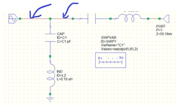
In case of high frequency, it is very sensitive to copper wire.
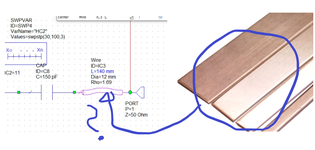
The actual product and the simulation result are very different.

so I want to apply a parasitic value to the element and the wire that the element is connected to in the circuit
Is this possible with AWR?

thank you so much for reading this.
happy new years.
 

Attachments

  • z.png
    z.png
    50.8 KB · Views: 112

This is a case where some amount of input resistance is required. It's needed for passive components to operate in their filtering role.

In real life there is some amount of input resistance. It might be present in circuitry upstream. Perhaps it's invisible and unknown. Regardless, it ought to be included in a schematic to show it's understood that input current is not infinite and is purposely limited to a reasonable level.

It's up to the designer to select the proper ohm value so that the filter performs as intended with your chosen L & C values.
Thanks for replying in advance
If it can't be applied to wire length, area, material properties, etc.?
 

PCB layout programs are mentioned in discussions at this forum, which calculate electrical characteristics of copper vias and how they interact in rf circuitry. Since I have no hands-on experience with these, perhaps one of our resident experts can tell you more.
 
I expect, "wire" refers primarily to PCB traces. Depending on the length, they can be either modelled as transmission line segments (length > lambda/10) or lumped series inductor and shunt capacitor. Transmission line impedance and capacitance/inductance can be obtained from PCB calculation tools. I guess you can use transmission dimensions in AWR directly like in ADS.
 
AWR have few models of bond wires placed over a ground plane. Search for BWIRES models.
 
I was able to solve it to some extent through a wire elemental, but Can't i model something like a copper plate like the picture?
 

Attachments

  • zc.png
    zc.png
    211.9 KB · Views: 96

I was able to solve it to some extent through a wire elemental, but Can't i model something like a copper plate like the picture?
To get more accurate results, I suggest you should probably model this system as a multiconductor transmission line (MTL), where the third conductor (your copper bar) is open-circuited at both ends. I assume AWR should have some MTL model, though I am not sure. You probably need to perform an electrostatic analysis or simulation to get the MTL properties of nonstandard lines such as this one.
 
Status
Not open for further replies.

Part and Inventory Search

Welcome to EDABoard.com

Sponsor

Back
Top