Continue to Site

Welcome to EDAboard.com

Welcome to our site! EDAboard.com is an international Electronics Discussion Forum focused on EDA software, circuits, schematics, books, theory, papers, asic, pld, 8051, DSP, Network, RF, Analog Design, PCB, Service Manuals... and a whole lot more! To participate you need to register. Registration is free. Click here to register now.

How Connect Pins of EPM7032SL(MAX 7000s Altera Series) for Programming?

Status
Not open for further replies.

panda1234

Full Member level 2
Joined
Jan 22, 2015
Messages
125
Helped
4
Reputation
8
Reaction score
4
Trophy points
18
Activity points
1,172
Hi,I bought Altera MAX7000s and a programmer but i don't know how to connect pins for programming please Help me.
in below picture you see MAX7000s and it's programmer:
Presentation1.jpgWP_20140522_001.jpg
 

Hi,I bought Altera MAX7000s and a programmer but i don't know how to connect pins for programming please Help me.
in below picture you see MAX7000s and it's programmer:
View attachment 115941View attachment 115942
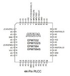
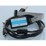
I think you may have been suckered into buying this stuff. The programmer is a clone of some sort of a byte blaster, which as far as I know a parallel port JTAG programmer (hope you have and old computer to go along with this antiqued part :wink:). The device in the PLCC carrier looks like the programming head for the older pre JTAG MAX7000s.

Can't read any of the markings on the MAX7000 so can't check it it's a new generation part with JTAG or not.
 

Its model is:EPM7032SLC44-10
W BFE320743A
 

The required JTAG connection can be found in the MAX7000S datasheet, the Byte Blaster JTAG connector pinout is identical to other Altera programmers (e.g. USB Blaster). As ads-ee said, needing a true LPT port may be a problem, the Byte Blaster doesn't work with most USB-to-LPT bridges.

The DIL adapter is intended as a breakout device for breadboards, I presume. Programming of non-JTAG MAX7000 is beyond the possibilities of a simple programmer circuit.
 

Looks like you're in luck it should be a JTAG part so you need to connect the programmer to the JTAG pins on the following diagram:
Capture.JPG

The ByteBlaster II look on page 2-3.

Just remember JTAG host connections almost always mean TDI connects to TDI on the target and TDO connects to TDO on the target. Don't try connecting TDI to TDO, that's only done when you are connecting the scan chain between devices.
 
Can you Stick numbers of pins should be connected in below picture:
WP_20150528_001.jpg
 

Everything in the original Altera Byteblaster manual.
 

Attachments

  • dsbyte.pdf
    354.3 KB · Views: 81
Thanks but i have a question in my above picture which pin is 1?
 

If the ribbon cable was mounted to the connector correctly (unknown if the cable was hand made) the red marking on the cable looks to be on the bottom so pin 1 is likely on the lower left (based on the cut off portion of the ribbon cable exiting to the right side of the connector).

Given this picture off ebay for a byteblaster has pin 1 where I said above....
mOzyO5MAQwMkniMLSv6H8cg.jpg

I think I'm correct in saying pin 1 is on the lower left corner of the connector in your photo.
 
Besides the red cable marking, lower left pin 1 position is also given by the key position of the IDC connector.
 
Status
Not open for further replies.

Part and Inventory Search

Welcome to EDABoard.com

Sponsor

Back
Top