Continue to Site

Welcome to EDAboard.com

Welcome to our site! EDAboard.com is an international Electronics Discussion Forum focused on EDA software, circuits, schematics, books, theory, papers, asic, pld, 8051, DSP, Network, RF, Analog Design, PCB, Service Manuals... and a whole lot more! To participate you need to register. Registration is free. Click here to register now.

How can I get rid of that noise?

Status
Not open for further replies.

beetlejuice

Member level 1
Member level 1
Joined
Jul 6, 2012
Messages
36
Helped
1
Reputation
2
Reaction score
1
Trophy points
1,288
Location
Melbourne Australia
Visit site
Activity points
1,799
Hi All

This is not really a FPGA, CPLD problem but there seemed no better place on the forum to ask for help.

I have a board that I designed about 8 years ago. Its a standalone framegrabber with Video decoder, FPGA, RAM etc and an AD7125 VGA driver. Its been working great for 8 years.
Now the SAA7111 video decoder is obsolete I have redesigned the board and changed to a TVP5146 video decoder. Now I have digital noise showing through on my vga output.

I'm not asking anyone to explain why I have noise because I know its a PCB problem, but something is really puzzling me ....

I have bypassed my local board power supply and have supplied the 3.3v circuitry form a bench PSU. I still see the noise. HOWEVER - I noticed if I turn the PSU voltage down to 3v the noise goes away. If I turn the PSU voltage up to 3.5v the noise goes away. But at 3.3v its the worse case of noise. It obviously seems to be some sort of resonance but I'm banging me head against the wall trying to get rid of this noise at 3.3v.

Does anyone out there have some knowledge/experience to share to help me figure out whats going on.
 

Do you know what frequency the digital noise is at, or is it more random?

The only thing that comes to mind based on changing the supply voltage using a bench supply would be that the I/O drivers of something on the board aren't impedance matched well enough and are probably over/under shooting and ringing and the change of the supply rail for the I/O is changing the characteristics of that ringing enough that you either see or don't see it in the vga output.

Were there any changes in the layout right around the AD7125? Especially the analog ground/power planes and the routing in layers above and below those planes?


Regards

- - - Updated - - -

Just took a look at your TVP5146, how is the layout of that part? Are any of the digital signals routed through the area where the ADC inputs are?

Just thought of something you might try, how about grounding the ADC VI_#_A/B/C inputs one at a time and see which one is coupling to the digital noise. You could ground between the AC coupling cap and the TVP5146 (probably at the via that connects to the TVP5146 pad or at the cap). If it turns out that you can get rid of the noise from the VGA output (of course you video probably won't look natural) then you can take a look at the routing around that input.

Regards
 

does your board continue to work at 3v and 3.5v ? Maybe something just stops working, and hence the 'noise' disappears.
 

Hi ads-ee

Thanks for taking the time to reply to my thread and far taking the time to look at the TVP5146 device. I'm working alone so its great to have someone to throw some suggestions into the pot.

The noise is random and very low level. Its not producing diagonal bars or anything like that what you get from Switcher PSU noise. The noise is in the pixels, but it does have some some structure coming through producing low level vertical flecks.

I have been working on it again this morning and have identified that I have 2 problems.

1. ADV7125

I can reduce the noise in some part by putting a 10ohm resistor in the supply to the adv7125. Previously there was a ferrite 60@100MHz, but changing that to a resistor helps. However the adv7125 is then working from 2.6v !!. I then took off the resistor and powered the adv7125 up from a separate 3.3v bench supply, with the common ground with the PCB but the noise is back, and this time the noise does not improve by reducing the voltage.

Odd thing is this part of the boards has not been changed so I think its not the real issue.

2. TVP5146

I have a camera connected up to the PCB and observed that even when the camera IRIS is fully closed there is still a low level dark noise on the screen. The camera is only just about 300mm from the board. I tool the signals from the camera Y/C and connected them directly onto the 75ohm input resistor on the TVP5146. There was no improvement. I powered the camera up from a separate 12v supply. Still no improvement. So I have this background noise even when the IRIS is closed, but if I drop off the Y signal it disappears. This suggests the noise is coming from the camera - BUT - I use exactly the same camera on the old board and no problem at all.
It seem somehow like the noise is coming in through the camera but I think this is also a false lead.

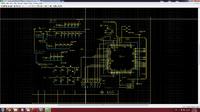
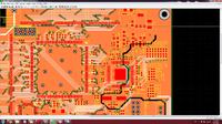
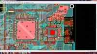
I have attached images board layout and schematic for the decoder part of the PCB.

The green layer is the power plane. The large 208PQFP is the FPGA. The chip to the right is the TVP5146. The ground around the decoder is split into +3.3digital, +1.8digital, +1.8analog and +3.3analog as viewed from left to right. The sot223 device above the TVP5146 is a 1.8v regulator.

The brown layer is the ground plane. I have split it under the TVP5146 and all analog circuitry is to the right of the split. The analog side of the ground plane extends down the right side of the board to the Y/C inputs connector. There is nothing else connected to this part of the ground plane.

Any thoughts would be greatly appreciated


If you split digital and analog ground, the single point of connection between them should be at the TVP5146. Look at the application example in the data sheet, section 5.1. The schematic suggests how the ground can be separated. Pins 26 (AGND) and 27 (DGND) should be directly tied together, that is the single point of connection. Ground planes are not discussed in the data sheet, but I suggest that you don't split the ground planes below the TVP5146.
Extend the "single point of connection" to the whole area occupied by the TVP5146.

It is easy to do more harm than good with ground splits.
 

Hi std_match

There is a PCB guidelines document for the TVP5146 https://www.ti.com/lit/an/slea079/slea079.pdf
The document shows to split the ground plane. I'm far from expert in PCB designe and am not sure how the analog and digital planes should be connected together. As you see from my layout I have just left a solid block of copper at the top right. To me this seemed sensible as there is nothing digital on the right (analog) side of the split so there should be no current flows to add noise to the signal.

I have since thought that my oscillator connection on the analog ground plane may cause currents straight up past the analog inputs and around to the digital side. I have since disconnected the oscillator caps from the analog side and bridged them onto the digital side - but the result is the same.


There are many previous threads about split ground planes respectively how to connect analog digital grounds.

You'll find split ground plane suggestions often with reference designs, that are in terms of existing mixed signal systems rather trivial boards, with only one mixed signal chip. The latest when a second mixed signal chips is added, you'll wonder where to connect the ground nets.

Except for special cases, a common continuozs ground is the best solution.
 

It's bad that the document doesn't mention where analog and digital grounds should be connected together. In my opinion, that should be done at the TVP5146.

You should read this:
http://www.hottconsultants.com/techtips/split-gnd-plane.html

I have just read the article and it all makes sense. I'm off to try to create some bridges over the ground plane split
I'll let you know if it helps

- - - Updated - - -

I've just tried bridging the ground plane. I used 5 wire links directly across the top of the TVP5146 from the analog GND to the Digital GND. I know its not as good as a solid ground plane connection but I would expect to see some improvement. The fact is - it did not make any difference at all !

I've attached an image of the noise I'm getting. Apologies for the very poor photo but the screen was just reflecting the camera unless i tilted it down. This is the screen I get when I completely close the iris on the camera, ie this is my background noise. You can see it has some structure of vertical lines so its not just random analog noise. By the way, the camera was also tested on my previous board and its not giving this problem on that board so I am assuming its not the camera that's producing the noise.

Its driving me nuts!


beetlejuice,

what is your board stackup?

I'm having trouble determining what the traces are that cross over the split in the ground plane. If these signals are not static they will induce ground currents who knows where. It's a really bad idea to pass any signals across a split ground plane as there isn't a return path anywhere nearby. You're return path in these situations will become the path of least resistance for the electorns, which is usually an undesirable path back.

You might also be seeing problems with return currents cutting through the power plane if that is the easiest route back. The split up power plane might be contributing to the problem if the reference plane for the signals passing across the splits is the split power plane layer.

Have you tried the grounding of VI_#_A/B/C inputs. That might tell you if the problem is injected into analog inputs.

Regards

- - - Updated - - -

Another observation on the "bluish" power plane picture. There is a series of parallel lines running across the top of the picture. That look to be tapped off in the middle of the trace between two destinations. Unless all these lines are static or nearly static you're signal integrity may suffer if they have the typical sub ns rise times of today's FPGAs. The long stub will result in reflections that will degrade your signals. Do you have access to a TDR to test these traces? You would probably be better off using fly-by routing as it will present a smaller discontinuity on the transmission line.

Regards

- - - Updated - - -

Was this board routed with an auto router?

Most of the good board designers (they mostly hand route boards) would not place vias like a fence across large stretches of the board like this:
Capture.PNG
This set of vias basically makes a large slot in the ground plane which means return currents have to go around the slot. The ground plane in this design is covered with these ground plane "slots".

Regards
 

ads-ee

The board stack up is Red is Top copper; Brown is Ground Plane; Greeny-Blue is Power plane; Blue is bottom copper

I see your point about the signals crossing over the ground plane split. I assume you are talking about the three vertical blue tracks. These are actually SDA, SCL, and RST for the TVP5146. And although i agree with your point i do not think these will be responsible for the noise. The SDA, SCL lines are only used once at start up to configure the device, after that they are static. Also the RST signal is only asserted at start up.

All the VI_#_ABC inputs are grounded. Thats the bank of 8 resistors and capacitors to the top right of the TVP5146.

Other tests to date ...

I have now connected 5 wire straps across the ground split at the TVP5146 by connecting the GND terminals on the decoupling caps on the analog side to the GND on the caps on the digital side. Although not an ideal ground plane connection I would expect to see some improvement in the noise level. However no improvement was seen at all.

I have also isolated the crystal circuit from the analog side and connected to the digital side, but no improvement.

I started to think it may be a digital issue in the FPGA, on the YCbCr bus. But the system uses embedded syncs and the sync is working flawlessly, which suggests that there is no data corruption on the bus. Additionally increasing the Luma Gain (Reg 47 in the TVP5146) causes the noise level to increase, so that absolutely convinces me the noise is at the Luma input.

Additionally I have done the following tests. Connect only the Luma input with Chroma removed. The noise is still present. Connect only the Chroma input with Luma removed. The image sync is affected as you would expect, but the chroma only image has no noise. So the noise source is definitely on the Luma signal. I check the signal with the Camera iris closed. The image should be black, but the background noise is visible. However, if I disconnect the camera from the Luma input then there is no noise! The TVP5146 continues to generate Hsync and Vsync signals under this condition, why is there no noise on the signal now ? It suggests that the noise souce is from the camera, however i do not have this problem with my previous board. I have also tried a different camera but with the exact same result.

I have been in touch with Texas instruments and asked "Is it possible that the noise is still present at the input of the TVP5146 when the camera is not connected, but the TVP5146 just forces black level in the absence of camera Luma, and sync signals? I presume this is the case." I am waiting for their reply.

Regarding your other comments on the PCB, I take it all on board and this has been a learning event for me. The board was routed manually by myself about 8 years ago, and its worked fine until this change to the video decoder, although the ground plane split is a new feature, as recommended by the TVP5146 app note. I'll continue to hack at it today and isolate the problem further

Thanks a lot for all your comments and assistance. It really is a great help.
 

As part of your learning experience try changing the breakout of a qfp to pairs of pins breaking out on alternating sides of the pads. That avoids creating a split in the planes due to the keepouts around the vias.

So you're saying the connection between the cap and the Luna input are grounded? Or were you referring to the unused ones? What I was suggesting was grounding an input like the Luna on either side of the series cap to see if it changes the noise. Depending on which side has an effect if any you might get a better idea if it's really the camera or something getting injected into the input after the blocking cap.

Regards
 

As part of your learning experience try changing the breakout of a qfp to pairs of pins breaking out on alternating sides of the pads. That avoids creating a split in the planes due to the keepouts around the vias.

Nice tip - will bear that in mind for the next time.

Regarding the inputs - I am using two inputs, Luma and Chroma. The other 8 inputs are connected to ground through 100nF capacitors and 75R resistors. I know the resistors are surplus to requirement.

On the input to the Luma I have the recommended anti alias filter a 75R termination and then 100nF ac coupling capacaitor. Exactly as shown on the evaluation module. See my schematic from earlier post

The main thing I get from my test are here ...

1) I have the Luma from my camera connected directly onto the input of the Y antialias filter. I mean directly through 150mm of wire onto the pad of the first inductor. I do not connect the Chroma signal. The noise shows up as it always has.

2)I have the Chroma from my camera connected directly onto the input of the C antialias filter. I do not connect the Luma signal. I still get unsynchronised Chroma signals on the screen but he noise is gone.

3)I disconnect both Chroma and Luma, i have nothing at all on the screen, and no noise.


Deductions are that the noise is only on the Luma signal, but then again would it actually be visible on the "abstract" chroma signals.
I think that the TVP5146 detects that the camera sync is missing and forces the YCbCr bus signals to 'black', hence the noise is masked. Waiting for TI to get back to me on this.

I bridged across the ground plans by connecting the grounds of the decoupling caps on the analog side to the decoupling caps on the digital side. Short wires were used strapping directly across the top of the chip. I have done this in 5 places and also solder linked the chip analog and digital ground pins 26 and 27. I expected to see some improvement, but there was no improvement to the noise at all, which suggests to me that the ground split is not entirely the cause.

I've used separate bench power supplies to power up the TVP5146 but no improvement. Actually i also took inductors out of the supplies to the TVP5146 but it did not get any worse. It just does not change no matter what i do with the tracks around the TVP5146, and thats bugging me so much, that I think its not down to the ground plane. I have 2 boards made up and both have the same issues, so its not a faulty chip.

The only thing that reduces the noise is reducing the 3.3v supply to the board to 3.0v at which point it is barely noticable. Also increasing to 3.5v reduces it significantly. I've tried applying this power supply variation to the TVP5146 alone, while the rest of the board remained at 3.3v but that made no difference at all, it just works when the whole board is reduced.
 

Regarding the inputs - I am using two inputs, Luma and Chroma. The other 8 inputs are connected to ground through 100nF capacitors and 75R resistors. I know the resistors are surplus to requirement.
I understand how you've connected this and the tests you've performed up to now.

What I'm suggesting is shown in the following diagram. Leave the camera connected to both C_IN and Y_IN.
Capture.PNG

I think it might be helpful to know if the noise is injected into the design between the cap and the TVP5146 or it's actually coming in before the cap. If Test 1 still has noise then the noise has to be coupling in after the cap, which means test 2 should have similar results to disconnecting Y_IN.

The only thing that reduces the noise is reducing the 3.3v supply to the board to 3.0v at which point it is barely noticable. Also increasing to 3.5v reduces it significantly. I've tried applying this power supply variation to the TVP5146 alone, while the rest of the board remained at 3.3v but that made no difference at all, it just works when the whole board is reduced.
If it's digital noise from the FPGA I/O switching then you might see a difference with differences in voltage. Can you isolate the FPGA I/O ring voltage and run that down to 3.0V? Could you try reducing the drive strength of your FPGA I/O to the minimum (default is probably something like 8 or 12 mA)? Running the I/O with a lower drive strength will reduce the magnitude of the reflections if there are any.

Regards
 

I've tried what you suggested. ie grounding before and after the input cap. In both cases the image is clean - solid black, however this is also the case when the Luma signal is disconnected. I think that the TVP5164 just forces black level output on the digital bus when it cannot detect the sync pulses on the Y input.

This morning I have put a saw cut through my board at the top of my analog ground plane so that my analog plane is now totally disconnected from the digital plane inside the PCB layers. The saw cut, above R58 to R62 effectively extends the slot in the ground plane out to the edge of the board. So now any any currents in the analog plane that need to get back to the digital plane can only get there via the ground links I have put directly across the top of the TVP5146. I have shorted the analog and digital ground pins at the chip. and strapped 5 short wire links from the analog side of the ground plane to the digital. This is the best i can do to simulate connecting the two planes directly under the chip. The result - no difference.

I have even lifted the xtal circuitry from the board and now rebuilt that on top of the chip. It was sitting over the analog plane so i removed it. I even cut the tracks to the crystal pads in case they capacitively couple into the analog plane. No difference.

I'm about to reconfigure the FPGA outputs for lower drive!
 

Previously in post #11 you mentioned this test with the Luma signal removed and the Chroma signal connected.
beetlejuice said:
Additionally I have done the following tests. Connect only the Luma input with Chroma removed. The noise is still present. Connect only the Chroma input with Luma removed. The image sync is affected as you would expect, but the chroma only image has no noise. So the noise source is definitely on the Luma signal.
Now you say the TVP5164 just forces black level output when removing the Luma input by grounding either side of the input cap...
beetlejuice said:
I've tried what you suggested. ie grounding before and after the input cap. In both cases the image is clean - solid black, however this is also the case when the Luma signal is disconnected. I think that the TVP5164 just forces black level output on the digital bus when it cannot detect the sync pulses on the Y input.
So I'm assuming in both cases the result was the TVP5164 forces a black level output when there is no Luma input. That wasn't clear from the description in post #11. I actually thought you were getting some output that wasn't sync'd but was clean, instead of a black level output.

From your previous tests and the current one I don't think you have a digital/analog ground plane issue. If you did then strapping should have changed the behavior.

Is there no way to isolate the I/O supply for the FPGA? It would be nice to know which component on the board that drops to 3.0V stops the noise. You've already ruled out the TVP5164...

Have you verified the input filter on the Y input has the correct component values?

Regards

- - - Updated - - -

Are you absolutely sure you don't have Chroma noise too?

https://forum.doom9.org/archive/index.php/t-159586.html
The fourth post has this to say about noise on the inputs..
So if you have noise in the Luminance, the picture looks noisy in a grayish way, like an old black and white move.
If you have noise in the Chroma, then the color looks unstable like an old VHS tape.

The noise in the luma is pretty much spot on. So are you seeing the color problems? Take a look at the thread on that doom9 site there are a couple of links to I guess some videos of noisy chroma.
 

Status
Not open for further replies.

Part and Inventory Search

Welcome to EDABoard.com

Sponsor

Back
Top