curtis.lesmeister
Newbie level 1
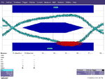
We have an in-house USB 2.0 high speed device design with a captive cable that is showing violations of the Template 2 requirements when measured at TP2 (host board connector). Specifically, we are violating the D+/D- Level 2 parameter values of -525 mV. (See attached waveform.)
Some other details:
After doing some on-line reading, I thought we might be able to correct it with a common mode choke, which I swapped in where the 0 Ohm resistors were. I tried several different values and used chokes specifically designed for applications such as USB 2.0, but none of them seemed to make a difference.
My questions are:
I am attaching a waveform of the eye diagram. My differential probe isn't the best, but when measuring eye diagrams of other high speed devices it has proved adequate to give a thumbs up to their performance.
Also, if anyone has any idea as to why the leading edge of the eye is weaker than the falling edge, I will take that input as well. We are not violating the eye, but I don't understand why there is a difference.
Some other details:
- this same device, with designed with a USB connector instead of a cable, passes with flying colors
- our captive cable measures about 8 inches, including the wire connection to the device
- the USB wires are broken out from the cable for about the last 3/4" before being direct soldered onto the device
- the USB lines do have ESD protection components, but there are virtually no line stubs
- we have 0 Ohm resistors in line with the USB D+/D- lines right after the solder connection to the device board
- the matched length of the D+/D- connection to the device component is about 1.5"
- when we insert a 6 ft. USB cable between the host and the device, the eye diagram smooths out and there is no longer a violation of the Level 2 parameter
- we very rarely see USB disconnects, and aren't sure if the ones we do see are unrelated to the eye diagram violation
After doing some on-line reading, I thought we might be able to correct it with a common mode choke, which I swapped in where the 0 Ohm resistors were. I tried several different values and used chokes specifically designed for applications such as USB 2.0, but none of them seemed to make a difference.
My questions are:
- what is the cause of this eye diagram violation?
- how do we fix it?
- since we may not be seeing disconnects, is there any other problem or damage that may result if we cannot fix it?
I am attaching a waveform of the eye diagram. My differential probe isn't the best, but when measuring eye diagrams of other high speed devices it has proved adequate to give a thumbs up to their performance.
Also, if anyone has any idea as to why the leading edge of the eye is weaker than the falling edge, I will take that input as well. We are not violating the eye, but I don't understand why there is a difference.