garypang
Junior Member level 2

- Joined
- Aug 4, 2011
- Messages
- 24
- Helped
- 1
- Reputation
- 2
- Reaction score
- 1
- Trophy points
- 1,283
- Activity points
- 1,461
Hi,
I have recently designed a 2 layers high speed flex circuits where top layer is the high speed trace and bottom layer is the ground plane.
I have designed the flex using microstrip method.
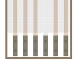
There are 2 variations of the design. One of them the soldering pad (for high speed trace >10GHz) is designed with via hole (see the attached image) and another one without.

From the measurement data for the transmission loss (S21) of the high speed trace, the design with via hole on soldering pad has much higher losses as compared to the one without.
Are there any way to compensate the losses caused by the via hole on the high speed trace? The via hole is used for simpler assembly during soldering process.
Thank you and hope that someone can provide your comment on this matter.
I have recently designed a 2 layers high speed flex circuits where top layer is the high speed trace and bottom layer is the ground plane.
I have designed the flex using microstrip method.
There are 2 variations of the design. One of them the soldering pad (for high speed trace >10GHz) is designed with via hole (see the attached image) and another one without.

From the measurement data for the transmission loss (S21) of the high speed trace, the design with via hole on soldering pad has much higher losses as compared to the one without.
Are there any way to compensate the losses caused by the via hole on the high speed trace? The via hole is used for simpler assembly during soldering process.
Thank you and hope that someone can provide your comment on this matter.
