Continue to Site

Welcome to EDAboard.com

Welcome to our site! EDAboard.com is an international Electronics Discussion Forum focused on EDA software, circuits, schematics, books, theory, papers, asic, pld, 8051, DSP, Network, RF, Analog Design, PCB, Service Manuals... and a whole lot more! To participate you need to register. Registration is free. Click here to register now.

High side switches not working as expectd

Status
Not open for further replies.

Hawaslsh

Full Member level 3
Joined
Mar 13, 2015
Messages
164
Helped
5
Reputation
10
Reaction score
7
Trophy points
1,298
Location
Washington DC, USA
Activity points
3,422
Hello,
AP2191 p-channel
BD2268 n-channel
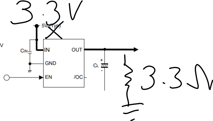
I have two high side switching I am experimenting with and in both cases I am not getting what I expect (good change my expectations are wrong). The pin out is different between the two parts, but they are connected the same, the picture below. I am using 10uF caps on the inputs and outputs, however, I get the same results with or without the caps. The load is a resistor in order to draw ~1A. To toggle the enable pin in both cases, I am using a wire to either short to ground or to Vin, 3.3V. In both cases my output voltage is ~2.5 V leading to a current draw of only ~750mA. Both datasheets claim on-state resistances of less than 200 mOhms so its confusing me to see such a voltage drop across the switch. Any suggestions or advice as to why these high-side switches are acting like this would be much appricated.

Thanks,
Sami
1633451880351.png
 

Hi,

show a photo of your circuit. (100kByte are sufficient)


Do you have a scope?

AP2191:
Did you properly connet the ceramics capacitor between IN and GND?
Connect EN to IN
Do measurements with a DVM.
connect DVM_GND directly to the AP2181_GND pin (not PCB)
do the measurements also at the according pins.
* measure EN
* measure IN
* mesure OUT

Tell us the values

Klaus
 

AP2191:
connect DVM_GND directly to the AP2181_GND pin (not PCB)
* measure EN
* measure IN
* measure OUT
1633466263799.png
1633466274180.png

Thanks for taking the time, apologies for the wall of text! I hope the pictures are sufficiently detailed. I am using the PMOS switch, AP2191. I performed the measurements above, and i made sure the DVM reference was connected to the GND pin (Not shown in the picture, the picture is measuring the voltage across the load resistor.)
On the breadboard: I performed the measurements with 2 different loads, 10K and 3 Ohms.
With the 10K load, everything is as expected. Vin = Ven = 3.3V and Vout = 3.3V
With the 3 Ohm load things are much different. Vin = Ven = 2.902V, Vout = 2.768. My power source is an Agilent E3631A and it is definitely NOT current limited, and still displays 3.3V. However, when I use the DVM to measure the output terminal of the E3631A, it was 3.137V with respect to the Chips GND pin. This lead me to measure the resistance of the cable connecting the E3631A to the breadboard, but it measured less than 0.2 Ohms.
The final test I did so far was to connect the 3 Ohm resistor directly across the E3631A using the same cable I've been using. This lead to a voltage across the resistor of 3.03V. The measured voltage at the E3631A terminal was 3.13V. I suppose that makes sense; 3.13V - (~1A *~.2Ohm) = 3.03V
Short summary: The switch seems to work just fine? But I am getting a large voltage drop from my power source to the bread board power bus. If i crank up the power source's voltage to ensure 3.3V at the bread board power bus, I get: Vin = Ven = 3.3V, Vout = 3.18V, current draw of 1.06A. The datasheet suggests a channel R of ~130mOhm at room temp; 3.3V - (1.06A * .13 Ohms) = 3.092. sufficiently close enough to my measured result.
One more question if you don't mind. The picture below illustrates what i planned on doing with the high side switch. I wanted to use a micro to power on / off a PLL chip in order to save power and perform a hard reset. My sever lack of foresight and planning forgot to include the voltage drop across the channel. Even if I design a great PCB with super low impedance paths to get 3.3V to the switch, the chip's max current draw of ~800mA will put the output voltage (3.3V - [0.8 A* .13 Ohms] = ~3.19V. Which is very close to the chip's minimum value for Vcc: 3.15V. Is there a better solution to this problem? I was only thinking of this part because it works with a micro (has its own driving circuity) and its packaging is nice and small. Perhaps just find a chip with a lower channel resistance? Thanks again!
1633467707362.png

1633468675468.png

I know there is a Chip Enable on the LMX2820 to power it down, but it doesn't perform a hard reset on the registers.
 

Hi,

Capacitors:
* in post#1 you said that these are 10uF, now you say they are 1uF.
Datasheet says:
* 0.1uF ceramics very close to the IC (I think yours is neither ceramics, nor 0.1uF, nor close to the IC)
* 10uF in parallel ...
There is a reason why they recommend this. You might understand or not why they recommend this, but you have to keep on this to get proper and reliable function.
Don't get me wrong: I'm not interested in to make you to feel bad, I want to get the circuit to work properly.

In post#1 the load is 3.3 Ohms, now it is 3.0 Ohms. Did you change it?

With the 3 Ohm load things are much different. Vin = Ven = 2.902V, Vout = 2.768
This is what I expected. Without knowing the reason when I wrote post#2.
Now I can imagine some reasons
* circuit may oscillate because of wrong capacitors / capacitor wiring
* a breadboard is not useful for the current and for short capacitor wiring. It introduces stray inductance which may lead to oscillations and it introduces ohmic resistance which causes voltage drop in input and (to) output

Good job! To the measurements you did, your calculations and your conclusions. Perfect.

*******

Your application:
The IC provides a 10mA power down mode. If you need to go below 10mA you have to cut it's power...this is your plan.
So far so good.
I see some possible issues.
* As written in the datasheet you need to follow the power up procedure strictly (timing, initialisation, internal calibration ....)
* You need to ensure that all signal inputs (SPI signals, other logic or clock signals...) are LOW during power OFF, otherwise the will feed power to the IC through the internal protection diodes. A very fail safe solution is to use analog switches on these lines.

Even if I design a great PCB with super low impedance paths
A pedantic not on this. It's not the "impedance" (in sense of HF) that causes the voltage drop, it's just the ohmic part.
While - in your case - low impedance is urgent for stability, low resistance is also urgent for low voltage drop.
The problem is: you can significantly lower the resistance by using wider and thicker traces, but the same is not true for the impedance.
Examples:
1) two traces, same length, same width, but one with 35um Cu, the other with 70um Cu
--> the thicke trace will have about half the resustance, but about identical impedance
2) two traces, same length, same width, same thickness, but one is routed over a solid GND plane, the other is routed over a split GND plane.
--> both will have identical resistance, but the one over the split GND plane will have much higher impedance

*****
Better solutions:
Indeed you may use any high side P-CH moset to switch power to the IC. But keep in mind to use slow switching and/or high value bulk capacitors at the supply side to reduce negative peak voltage drop when you swith power ON to the IC. There are very small logic gate P-Ch Mosfets with very low R_DS_ON.

Another option:
Consider to use a dedicated voltage regulator with ENABLE feature for the IC. It's regulation loop should keep voltage very accurate and stable.

Klaus
 

    Hawaslsh

    Points: 2
    Helpful Answer Positive Rating
Not all capacitors, for same capacitance, have same ESR -

1633514892293.png


Regards, Dana
 

Don't get me wrong: I'm not interested in to make you to feel bad, I want to get the circuit to work properly.
I come here for the good, the bad, and the ugly. All critics are welcome and appreciated! Thank you for taking the time to help!
Consider to use a dedicated voltage regulator with ENABLE feature for the IC. It's regulation loop should keep voltage very accurate and stable.
Fantastic solution.
--- Updated ---

Not all capacitors, for same capacitance, have same ESR -

Regards, Dana
Thats why i used the military spec, spaced rated, 6 dollar a pop ceramic caps. M39014/02-1411. Our stockroom is full of them, not sure why.
 
Last edited:

Hi
Thats why i used the military spec, spaced rated, 6 dollar a pop ceramic caps. M39014/02-1411. Our stockroom is full of them, not sure why
It's expensive, for sure good quality regarding failure rate.
But this dose not necessarily mean that it is suitable regarding electrical specifications.
Frequency range, ESR, series inductance, value drift...

Klaus
 

Status
Not open for further replies.

Part and Inventory Search

Welcome to EDABoard.com

Sponsor

Back
Top