Continue to Site

Welcome to EDAboard.com

Welcome to our site! EDAboard.com is an international Electronics Discussion Forum focused on EDA software, circuits, schematics, books, theory, papers, asic, pld, 8051, DSP, Network, RF, Analog Design, PCB, Service Manuals... and a whole lot more! To participate you need to register. Registration is free. Click here to register now.

High side IGBT damaging

Status
Not open for further replies.

jagdeepsingh3@hotmail.it

Member level 3
Joined
Sep 2, 2012
Messages
54
Helped
1
Reputation
2
Reaction score
2
Trophy points
1,288
Activity points
1,634
High side IGBT damaging 2 switch forward converter

Hello guys i want to ask few things:
1: how to calculate resistor and capictor values of snubber circuit.
2: i'm testing this circuit and with 60v on output and 6.5 ohm resistive load the high side mosfet burns could someone please help me?

sorry for my bad english.

thanks
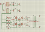
Cattura.PNG

- - - Updated - - -

some mistakes:
1: high side and low side igbts burns i checked it now

and here are some waveforms coming from hcpl-3120
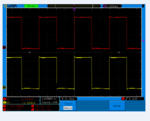
Cattura1.PNG
 
Last edited:

You will need some dead-time to prevent cross-conduction spike failures. Examine timing overlap and control the difference in rise fall time of Vgs with >0.5us no load, which reduces with loading..
 

You will need some dead-time to prevent cross-conduction spike failures. Examine timing overlap and control the difference in rise fall time of Vgs with >0.5us no load, which reduces with loading..

Hello sir thanks for answering
this is is a 2 switch forward converter.
i measured the rise time and fall time with igbt connected
Rise time: 180nS
Fall time: 460nS
20150128_752716.png
 

Its a half bridge diagonal forward converter running at 50% duty cycle, so dead time is not an issue.

It does seem to be working rather hard for IGBTs , over nine amps and 50Khz. Both switching and conduction losses are going to be significant.

Try experimentally running it at a much lower frequency say 5Khz and see if it still tends to burn up. At least that might tell you something.

It may be worth looking at using mosfets for this instead of IGBTs, the tradeoffs might be in your favour, especially at sixty volts, and even at much higher voltages.
 

I just noticed that the optoisolated drivers have Vee coupled to each Tblock pin2 which are each respectively connected to V+out and V-out.

If these driver power sources are floating then the IGBT output rails would also be floating and thus have no means of sharing the half cycle load.

If they are not floating then are they tied to the outputs as bootstrap supplies? That wont fly.

So what determines the floating reference voltage for each polarity?

A series 100mV drop current shunt may help debug the dynamic loss in the IGBT, while lowering commutation rate. Is the load just across the outputs or referenced to Bus in+\-.

Monitor V,I on each side of half bridge and offset with respect to Bus in-.
 

Its a half bridge diagonal forward converter running at 50% duty cycle, so dead time is not an issue.

It does seem to be working rather hard for IGBTs , over nine amps and 50Khz. Both switching and conduction losses are going to be significant.

Try experimentally running it at a much lower frequency say 5Khz and see if it still tends to burn up. At least that might tell you something.

It may be worth looking at using mosfets for this instead of IGBTs, the tradeoffs might be in your favour, especially at sixty volts, and even at much higher voltages.

I just noticed that the optoisolated drivers have Vee coupled to each Tblock pin2 which are each respectively connected to V+out and V-out.

If these driver power sources are floating then the IGBT output rails would also be floating and thus have no means of sharing the half cycle load.

If they are not floating then are they tied to the outputs as bootstrap supplies? That wont fly.

So what determines the floating reference voltage for each polarity?

A series 100mV drop current shunt may help debug the dynamic loss in the IGBT, while lowering commutation rate. Is the load just across the outputs or referenced to Bus in+\-.

Monitor V,I on each side of half bridge and offset with respect to Bus in-.

Hello guys first of all thanks for helping me.

i changed igbts this time i'm using G30n60a they were used in a inverter welding machine with 50khz frequency so i'm sure that they will work with hard switching.
this time output volt is: 50.5v
output current is: 7.65A

Input Bus dc voltage is: 300v
Bus dc current is: 1.810A
Here are some waveforms on transformer leads:
1: No load
no load 1.png

2: No load ring voltage:
no load ring voltage.png

3: No load ring time
no load ring time.png

4: With test load:
with load.png

5: with load ring voltage:
with load ring voltage.png

6: with load ring time is equal to no load time

with this load the igbt body temprature rises to 50C in 20-30 seconds and still increasing i don't know why...

- - - Updated - - -

D29 - 32 are all the wrong way round....

hello sir R40,R41 are RGon resistors and R46,R47 are Rgoff resistors this is reason :)

i hope it's correct
 

I will stick my hand up and support Orson.

Its far more usual to try to slow down turn on, and speed up turn off.
The gate drive circuit as drawn does it the opposite way.
Its a detail I missed.

I don't think it will make any difference to your temperature rise problem.
Its still rather a lot of power, what heat sinks are you using ?
 
Last edited:
I will stick my hand up and support Orson.

Its far more usual to try to slow down turn on, and speed up turn off.
The gate drive circuit as drawn does it the opposite way.
Its a detail I missed.

i did in this way because in some design notes i read that slowing the turn off it will decrease the switch turn off voltage spike....
and is there is anything thanks in not ok in my waveforms ?
please help sir thanks
 

You won't have any problems with turn off spikes because the IGBTs are clamped to the supply rails via D17 and D18.

Likewise you don't need slow turn on because with this topology you cannot get cross conduction if the duty cycle is limited to 50% as it is here.

Probably best to run full available gate speed.
From memory the 3120 output current is two amps, so just a single ten ohm resistor in each gate should be about right.

i'm going to try with only 10ohm resistor and i will let you know in few minutes what is changed..
thanks for helping

- - - Updated - - -

I just tried with only 10 ohm resistor and everything is same and igbt's body temprature reaches 50-60C in a few seconds please help i'dont now what is causing this
 

Likewise you don't need slow turn on because with this topology you cannot get cross conduction if the duty cycle is limited to 50% as it is here.

Slow turn on may be still required to control diode commutation and limit diode overvoltage.

I don't think that it's obvious at first sight which mechanism causes IGBT damage in this circuit, can be both overvoltage and dynamic overload during switching. Preferably you'll try to measure IGBT voltage and current waveforms, don't know if you have the necessary tools.
 

The diodes should be well out of conduction, as flyback duration will always be less than conduction duration, even at zero load.
Waveform "4" above bears that out.
Hence cross conduction can never occur even under the worst case no load condition.

Difficult to tell if this is switching loss or conduction loss, or just lack of overall heat sinking capacity.
 

The diodes should be well out of conduction, as flyback duration will always be less than conduction duration, even at zero load.
I see, it's true at least for forward converter steady state. I wonder if continuous conduction may still occur as transient state with DC welder rectifier load.
 

Possibly, with some weird reflected transient load.
But the diagonal half bridge is a beast with some unique and very friendly properties.
 

Sounds like the optos have not enough peak current to charge Cg of the IGBTs.
Try using another driver circuitry.
 

Sounds like the optos have not enough peak current to charge Cg of the IGBTs.
Try using another driver circuitry.

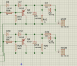
this is my new circuit for driving igbts, i was using this but the waveforms were distorted:
Cattura 11.PNG

- - - Updated - - -

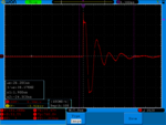
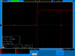
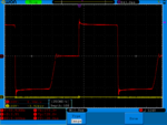
hello guys i managed to get a better snubber values and now the waveforms are:

1: No load
primo.png

2: With 350 watt resistive load
secondo.png

3: gate signal no load:
terzo.png

4: gate signal with 350 watt load (voltages of gate signal are wrong because the probe was on 1x sorry about that)
quarto.png

but 4 igbts (60A) per side are getting very hot with only 350 watt load why?:bang: help me guys...
 

How much effort have you put into predicting the conduction and switching losses in the IGBTs? Have you included losses induced by reverse recovery of the clamp diodes? Have you measured your actual efficiency? What's your expected thermal impedance on the IGBTs?
 

How much effort have you put into predicting the conduction and switching losses in the IGBTs? Have you included losses induced by reverse recovery of the clamp diodes? Have you measured your actual efficiency? What's your expected thermal impedance on the IGBTs?

i don't have instruments to measure switching and conductions losses in the igbts, but i tried to calculate the efficinecy with measuring dc bus voltage and currente and output voltage and current and it's about 70% like expected from a forward converter.
 

Static IGBT losses for new part can be modelled as Vce*Ice=P=(1.25V +0.01Ω*Ice)*Ice.

Thermal Resistance is unknown for your heatsink and interface, while Rjc is only 0.27'C/W Do you have a CPU heat sink?

Is this a bipolar output with centre ground load?
That would explain the asymmetric pulse widths to mid-level Voltage.

Drivers need to be able to transfer Gate charge ~1mJ or current limit of Ig x transition time. The test parameters used Rg=3, so driver ESR must be examined and // IGBT's factored.

ESR is usually 10x Rb for a saturated driver switch. where Rb is 330R?
Better ones are up to 50xRb, based on Vce(sat) Ic/Ib rating.

my rule of thumb is to compare impedance gain of each stage , working backwards.
I start with RL/RdsOn>100 , 6.5/0.01=650 ok
then RL/Rg>=5, you are <<1 with Rb=390//1k for Ib
Then Ic/Ib=10 or as rated , your gate drive is still too low.
 

Status
Not open for further replies.

Part and Inventory Search

Welcome to EDABoard.com

Sponsor

Back
Top