Continue to Site

Welcome to EDAboard.com

Welcome to our site! EDAboard.com is an international Electronics Discussion Forum focused on EDA software, circuits, schematics, books, theory, papers, asic, pld, 8051, DSP, Network, RF, Analog Design, PCB, Service Manuals... and a whole lot more! To participate you need to register. Registration is free. Click here to register now.

Help with ic layout design

Status
Not open for further replies.

tompham

Full Member level 2
Joined
May 29, 2010
Messages
133
Helped
29
Reputation
60
Reaction score
29
Trophy points
1,308
Location
usa
Activity points
2,066
Hi

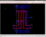
I have layout of complex function out = (AB+C)D . The DRC show no error but LVS show : Terminal "G" on device /+7 should be connected to /Cb instead of /Db (deivce +7 is pmos). I cannot figure out the error and need some help. Please help me with this. Thanks a lot.
 

Attachments

  • Screenshot at 2012-05-19 16:41:38.png
    Screenshot at 2012-05-19 16:41:38.png
    58 KB · Views: 58

Hi Keith

Thanks for your reply. I am new bee to ic layout and need your help. I still can not clear about your answer. Do I make mistake on pmos ? I still can not figure out

how. Please help me. Thanks

tom
 

I am simply commenting on the labels on the layout (you haven't shown your schematic). Assuming the LVS uses the labels then the labeling error will cause a problem.

Keith
 

Status
Not open for further replies.

Part and Inventory Search

Welcome to EDABoard.com

Sponsor

Back
Top