Continue to Site

Welcome to EDAboard.com

Welcome to our site! EDAboard.com is an international Electronics Discussion Forum focused on EDA software, circuits, schematics, books, theory, papers, asic, pld, 8051, DSP, Network, RF, Analog Design, PCB, Service Manuals... and a whole lot more! To participate you need to register. Registration is free. Click here to register now.

Help with differential usb 2.0 trackinginin

Status
Not open for further replies.

Rajinder1268

Full Member level 3
Joined
Mar 20, 2021
Messages
162
Helped
1
Reputation
2
Reaction score
4
Trophy points
18
Activity points
1,228
Hi all,
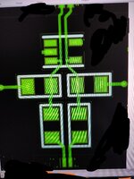
I have attached a tracking layout for USB 2.0 layout. I need some advice on how I can better this. So it comes from the USB connector, through a ESD clamp, through R C for signal integrity / termination them to the USB to UART device.
My questions:
1. I need to keep the tracking the same i.e. in parallel with a gap of 0.2mm and 0.2mm track width. I am struggling to get this.
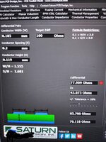
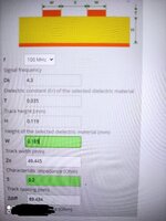
2. Also I am getting different results from USB impedance calculator. (See attached)
3. If we run at 480Mbps, will I have any issues with the current tracking?
4. I have right angles going into the clamp IC, i know it is not ideal but what is a workaround?

Thanks in advance
--- Updated ---

Here are the impedance calculator results.
 

Attachments

  • IMG_20210611_192017.jpg
    IMG_20210611_192017.jpg
    5.6 MB · Views: 199
  • IMG_20210611_193416.jpg
    IMG_20210611_193416.jpg
    7.7 MB · Views: 187
  • IMG_20210611_193453.jpg
    IMG_20210611_193453.jpg
    8.3 MB · Views: 190

You should target a higher Zdiff, 90 ohm +/- 10%. For top layer traces you should have continuous GND under the traces, do not cross any gaps in GND plane. Consider tuning your R-C components empirically using a USB 2.0 eye diagram test setup, and consider tuning using L-C instead of R-C to tune, use only high-Q wirewound inductors. Make sure to put local capacitor for your ESD array, adjacent to the array or on bottom side connected thru good vias. Connect the tuning C to top side GND plane instead of those small traces with vias, or good vias to inner GND very close to the C pads. I assume that is the TI ESD array, they have a SOT version with more space between the pins which may give you better layout option, using a slightly wider trace may get you closer to ideal Zdiff.
Do not worry about the right angles going to the ESD array, those are far too short to act as RF stub at fundamental (240MHz) and most important harmonic (720MHz). I would be more worried about the trace Zdiff and the manner in which you are connecting your tuning C to GND.
In the past I have favored wider traces sacrificing Zo for better Zdiff but USB 2.0 design is highly subjective due to the wide variance in USB transceiver characteristics between manufacturers (and even between different transceiver designs from the same manufacturer). This is why eye diagram testing is so critical for USB designs.
If you have a transceiver from Microchip(SMSC), Freescale, etc, your USB PHY likely has tuning options in software which will also help.
 

Status
Not open for further replies.

Similar threads

Part and Inventory Search

Welcome to EDABoard.com

Sponsor

Back
Top