Continue to Site

Welcome to EDAboard.com

Welcome to our site! EDAboard.com is an international Electronics Discussion Forum focused on EDA software, circuits, schematics, books, theory, papers, asic, pld, 8051, DSP, Network, RF, Analog Design, PCB, Service Manuals... and a whole lot more! To participate you need to register. Registration is free. Click here to register now.

help with combline filter in ADS

Status
Not open for further replies.

sandeepsreeman

Member level 1
Joined
Mar 28, 2009
Messages
33
Helped
0
Reputation
0
Reaction score
0
Trophy points
1,286
Location
india
Activity points
1,524
plz help

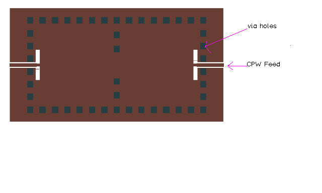
hi i designed combline bandpass filter in layout of ads one problem iam getting is how to make a via hole from stipline to ground and how to measure the hole dimensions to make that strip to connect to ground plane help in this aspect
 

plz help

Project Manager - Model/Via,press right button of mouse -Add Hole。then
input circle center(0,0) ,click the circle hole change its property radius and set it to be 2.5D
choose Planar EM in property window,
change BottomLayer to be
Gnd
that is all
 

Re: plz help

xue_xd said:
Project Manager - Model/Via,press right button of mouse -Add Hole。then
input circle center(0,0) ,click the circle hole change its property radius and set it to be 2.5D
choose Planar EM in property window,
change BottomLayer to be
Gnd
that is all
can explain step by step or little bit clear?
 

plz help

i am not right ,i thought what you use iwas designer,but you use ADS
best wishes
 

Re: plz help

Hi,

in Momentum layout window, first of all you must draw your hole. Chose a layer (for example the "Hole" layer) and draw it. Depending on the frequency, and on the amount you have to simulate it, you may want to draw it circular or poligonal. Most of the time, a square cross section is adequate. The dimension of the square will be almost the same of the circle you are aproximating.

When you are satisfied with your via hole, go to Momentum -> Substrate -> Create/Modify.. Menu. You have two tabs. In the first (Substrate Layers), you have to define the Dielecric layers of your design stackup. Once your dielectric layers have been defined, go to the second tab (Layout Layers). will have your dielectric layers interleaved with "-------" symbol. This is the metal layer of your PCB. Map the metal layer you used in the layout design to the right position in the stackup. Selectin a substrate layer you can map the holes as "Via" (Button in the bottom. Sabe and simulate.

The momentum Help can give you better insight on the differences between lumped, 2D or 3D via model, as well as how to manage thick metal expansion.

Good luck.

S.
 

Re: plz help

chemic said:
Hi,

in Momentum layout window, first of all you must draw your hole. Chose a layer (for example the "Hole" layer) and draw it. Depending on the frequency, and on the amount you have to simulate it, you may want to draw it circular or poligonal. Most of the time, a square cross section is adequate. The dimension of the square will be almost the same of the circle you are aproximating.

When you are satisfied with your via hole, go to Momentum -> Substrate -> Create/Modify.. Menu. You have two tabs. In the first (Substrate Layers), you have to define the Dielecric layers of your design stackup. Once your dielectric layers have been defined, go to the second tab (Layout Layers). will have your dielectric layers interleaved with "-------" symbol. This is the metal layer of your PCB. Map the metal layer you used in the layout design to the right position in the stackup. Selectin a substrate layer you can map the holes as "Via" (Button in the bottom. Sabe and simulate.

The momentum Help can give you better insight on the differences between lumped, 2D or 3D via model, as well as how to manage thick metal expansion.

Good luck.

S.
in the below fig i know how to draw the struture and .can u explain how can i make via ?i need ADS steps. i can make feed by using chop option i can remove undesired portion
 

Re: plz help

Let us suppose that you have three metal layers, and you map them to pc1, pc2 and pc3. If pc1 is the TOP ground plane and pc2 is the bottom one, you need two layers of vias to interconnect them, one going from pc1 to pc2 and another going from pc2 to pc3. So you will copy your squares on (let's say) pcvia1, pcvia2 and to pc2 as well, as they need metal interconnection in that layer to do a trough hole.
Then you go to th emenu I was describing before and map the right layer to the right place.
 

Re: plz help

chemic said:
Let us suppose that you have three metal layers, and you map them to pc1, pc2 and pc3. If pc1 is the TOP ground plane and pc2 is the bottom one, you need two layers of vias to interconnect them, one going from pc1 to pc2 and another going from pc2 to pc3. So you will copy your squares on (let's say) pcvia1, pcvia2 and to pc2 as well, as they need metal interconnection in that layer to do a trough hole.
Then you go to th emenu I was describing before and map the right layer to the right place.
good i am making via holes in silcondioxide there is no top metal layer can u explain how can i draw or make via ?i need ADS steps
 

Status
Not open for further replies.

Part and Inventory Search

Welcome to EDABoard.com

Sponsor

Back
Top