Continue to Site

Welcome to EDAboard.com

Welcome to our site! EDAboard.com is an international Electronics Discussion Forum focused on EDA software, circuits, schematics, books, theory, papers, asic, pld, 8051, DSP, Network, RF, Analog Design, PCB, Service Manuals... and a whole lot more! To participate you need to register. Registration is free. Click here to register now.

Help to understand an element in a schematic diagram.

Status
Not open for further replies.

szkot

Newbie level 2
Joined
Jan 10, 2014
Messages
2
Helped
0
Reputation
0
Reaction score
0
Trophy points
1
Activity points
17
Hi


I would like to learn to read schematic diagrams. On the following image


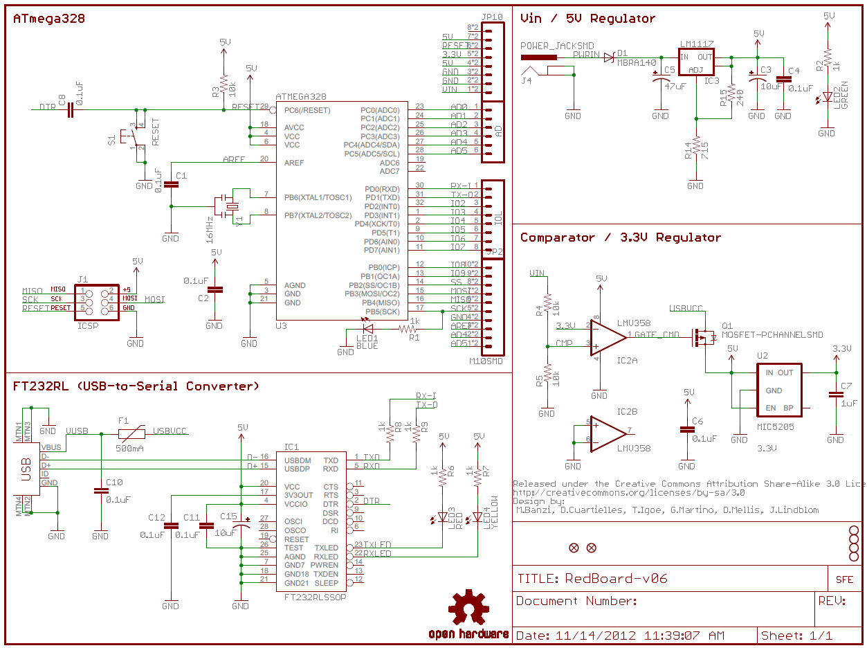
in the functional block 'Comparator /3.3 V Regulator' there is an element LMV358 with an output marked with the number 7. What is the aim of that element? How should it be placed in the diagram ie. what should the pin 7 be connected to?

Thank you for replies
szkot
 

LMV358 is a dual operational amplifier. In this circuit one Opamp(IC2A) is used as a voltage comparator and other(IC2B) is not used for any purpose. But the input of the other opamp is shorted to ground because of unwanted noise pick up.
 

LMV358 is a dual operational amplifier. In this circuit one Opamp(IC2A) is used as a voltage comparator and other(IC2B) is not used for any purpose. But the input of the other opamp is shorted to ground because of unwanted noise pick up.

Thank you for your response. Is there any reason that the designer have placed Opamp IC2B (not used) on the diagram? I come from the world of programmers and would like to understand how electronic designers create their diagrams.

Cheers
szkot
 

LM358 is an IC with dual opamp in it. In the schematics, he used only one opamp. But definitely the two have to be placed since it is a single part.
 

Thank you for your response. Is there any reason that the designer have placed Opamp IC2B (not used) on the diagram? I come from the world of programmers and would like to understand how electronic designers create their diagrams.

Cheers
szkot

No reason. But some case people using dual opamp instead of single opamp are given below
• May be considered for future application.
• May be dual opamp is cheaper and easily available compared to single opamp.

I come from the world of programmers and would like to understand how electronic designers create their diagrams.

Circuit diagram creating based on basic design. Electronic designers using EDA tools for creating circuit diagram
 

Is there any reason that the designer have placed Opamp IC2B (not used) on the diagram?
That is unusual. Certainly one would expect the designer to use a single opamp if only one is needed.

However for a manufacturer there may be other practical considerations. For example if they already make several other products that use LM358s, then it could make sense to just use more of the same, rather than something else. You get a much better price when ordering in bulk than you do ordering small quantities.

i.e. It's simpler and cheaper to order 10000 of one part rather than a few thousand of this, a few hundred of that, and 25 of something else. Makes stock control easier too.
 

If the only op amp available is the dual (perhaps they have thousands stocked and for 1 product getting in a new part is more costly than using the dual device), then it is important to ground one input for EMC purposes as stated above.

This requires that it is added to the schematic.

Additionally, it makes it so that the schematic reader is aware that this gate of the IC is not used, that the unused pins shown have nothing on them and what they do.

Its an improvement on the old ways of not showing them and good practise.

What is bad practise is that in the schematic there are several junction points with 4 connections on them, the max should only be 3.
 

Status
Not open for further replies.

Part and Inventory Search

Welcome to EDABoard.com

Sponsor

Back
Top