Continue to Site
Follow along with the video below to see how to install our site as a web app on your home screen.
Note: This feature may not be available in some browsers.
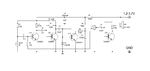
Could you tell me how to create the schematic diagram?
I ask myself: why?Here the design that I want to reproduce
Can you help me to identify the parts? I am a student... (beginner). Thanks, Anne
What about only a Gerber file?