allennlowaton
Full Member level 5
Good day guys..
Please help me with these..
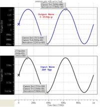
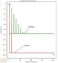
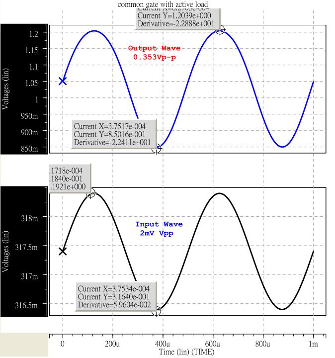
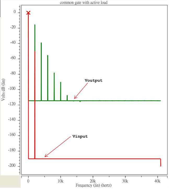
I'm doing a common gate with an active load. During transient analysis, the output wave with respect to time looks fine. But in the FFT analysis, the output wave generates many harmonics.
My concerns are:
1. I'm curious on what happens in the inside of the common gate (in this case) that causes these harmonics to pop out. What's the circuit that causes them?
2. Why is the level of output compared with the input in the FFT graph is higher? What causes this difference in level?
Attached are the following:
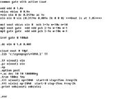
My .SP code
Transient Results
FFT Analysis Results
Thank you very much for any help.
Added after 3 minutes:
sorry, concern number 1 should be like this:
1. What's in the circuit that causes harmonics to be generated.
Thank you...
Please help me with these..
I'm doing a common gate with an active load. During transient analysis, the output wave with respect to time looks fine. But in the FFT analysis, the output wave generates many harmonics.
My concerns are:
1. I'm curious on what happens in the inside of the common gate (in this case) that causes these harmonics to pop out. What's the circuit that causes them?
2. Why is the level of output compared with the input in the FFT graph is higher? What causes this difference in level?
Attached are the following:
My .SP code

Transient Results
FFT Analysis Results
Thank you very much for any help.
Added after 3 minutes:
sorry, concern number 1 should be like this:
1. What's in the circuit that causes harmonics to be generated.
Thank you...