Continue to Site

Welcome to EDAboard.com

Welcome to our site! EDAboard.com is an international Electronics Discussion Forum focused on EDA software, circuits, schematics, books, theory, papers, asic, pld, 8051, DSP, Network, RF, Analog Design, PCB, Service Manuals... and a whole lot more! To participate you need to register. Registration is free. Click here to register now.

[SOLVED] Help needed in designing a discrete circuit

Status
Not open for further replies.

explorick

Advanced Member level 4
Joined
Jun 14, 2006
Messages
109
Helped
8
Reputation
16
Reaction score
3
Trophy points
1,298
Activity points
2,037
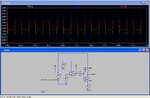
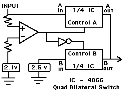
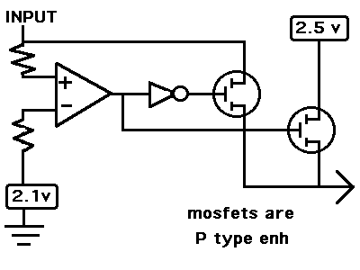
There is a variable voltage coming as Vin which can be vary between 3.3 and 1.1V. For Vin voltages between 3.3 to 2.1V the output should be 3.3 to 2.1V, for voltage less than 2.1V the output should be fixed at 2.5V. For this i created a circuit and was not successful with it because the body diode of PMOS is conducting when control voltage is high. Is there any other circuit you could suggest. I cannot use diode in the Vout path as that would add drop. The circuit an observation is as attached.
 

Attachments

  • untitled.JPG
    untitled.JPG
    70.5 KB · Views: 101

The N-mosfet appears to be reversed source-for-drain. (That is, going by its symbol on the schematic.)

Perhaps you installed it correctly on the circuitboard. There remain questions.

An N-mosfet has its gate referenced to the source pin (the more negative pin). Yet it's not clear what polarity its source is. What should current direction be when the N-mosfet is conducting? Does it have a path through any load connected to the wire labelled 'output'?

A P-mosfet has its gate referenced to the drain pin (the more positive pin). There are similar questions as for the N-mosfet.

Another question: Did you intend for there to be any time when both mosfets are conducting?
 

... the body diode of PMOS is conducting when control voltage is high. Is there any other circuit you could suggest.
What about setting M1's source/bulk voltage to a fixed vdd of 3.3V ?
 

@BradtheRad: When there is no Vin. The opamp will drive high and the NMOS conducts which would give 2.5V.When Vin exceeds 2V the opamp will drive low and the PMOS will give 3.3V output. The current will be to the load connected to the Vout pin. The direction is from 2.5V supply to Vout pin.The PMOS is referenced to Source pin with 3.3V and its not drain pin.
At any time only one FET will be conducti
@erikl: Whatever voltage coming as Vin should be fed as a supply to the load. The voltage is not constant at 3.3V. If it is constant the concept of PMOS body diode conduction will not come at all.
 

I think I see now. It's a matter of selecting one of two analog signals.

The 4066 Quad bilateral switch is suitable. It's very much like a relay. Its internal structure has mosfets arranged a little more complicated than your circuit.

81_1317643508.gif


I use the 4066 to switch rapidly between two signals going to my oscilloscope. The inputs/outputs don't seem to care what V the signal is, or whether it's AC or DC.

The control pins respond to logic level signals. When a control is low, then its related output pin is high impedance. When the control is high, internal mosfets connect the output to the input with 80-250 ohms intervening.

Not sure you'll need to put input resistors at the op amp. I drew them in just in case.

This may need some adapting, depending on your supply configuration.

If you use single supply, then consider using a comparator instead of an op amp. The comparator's output will go to either hi-impedance or ground. In order to make output high you'll need to add a pullup resistor.
 

Thanks for your suggestion. The load current requirement is 0.5A and the onresistance provided by these devices are too high to use. If I use relay the size might be too big. So i thought of using Mosfets.
Also what is the advantage of using comparator IC instead of Opamp. If I choose a rail to rail output opamp the output can drive till 5V or 0V considering 5V supply which is maximum voltage in my design. Also my plan is to have a configurable schmitt trigger circuit around opamp if needed.
 

There's no reason you can't use a single supply op amp.

Going back to your original circuit. It may work by using two P mosfets, with an inverter added. The inverter might be replaced by a transistor in the right configuration.

A P-mosfet gate is referenced to the drain terminal (closest to positive). By sending 5V to the gate, it will make the device shut off.

By pulling the gate to ground, it should pass whatever voltage is present at the upper terminal. This is 2.5V at one mosfet. It may or may not turn on the mosfet sufficiently to give you the .5 A you specified.

Similarly with your incoming signal voltage. May or may not be sufficient.

Could be worth a try.

62_1317756860.gif
 

A P-mosfet has its gate referenced to the drain pin (the more positive pin).
No. Both P-mos and N-mos have their gates referenced to source. And the more positive pin on the P-Mos is the Source.
 

No. Both P-mos and N-mos have their gates referenced to source. And the more positive pin on the P-Mos is the Source.

Looks like they've perpetuated the confusing nomenclature that also had me confused with transistors for the longest time.

And then there was the idea that JFETs can be switched drain for source. Even though the pins are labelled D and S.

Source should mean source of electrons, or rather that's why I thought they wanted to start using a different name than emitter. Seems confusing enough to call a PNP transistor emitter the emitter even though it doesn't emit electrons.

My habit is to test such components with my ohmmeter set on high range. That way I know I'm orienting it properly.

As you state, a P-mosfet ordinarily operates with its gate referenced to the more positive pin.
 
Last edited:

As per my knowledge, the design will not work even with two P Mosfets because the body diode conduction will happen in this case also.
 

the design will not work even with two P Mosfets because the body diode conduction will happen in this case also.
True. But what if you replace the input PMOS by a power pnp BJT ? There should be no reverse conduction, I think. Probably its base control has to be adapted a bit. The forward drop could be similar to a PMOS'.
 
Then I can think of a complementary BJT instead of CFET. If the Vce sat is below 125mV it will work for me. I was in an assumption that the minimum VCE sat will be around 0.3V. So i didnt proceed with BJTs, but now i found device(Zetex -ZXTC2061E6 ) which matches my requirement. Thanks for the suggestion.
 

Status
Not open for further replies.

Similar threads

Part and Inventory Search

Welcome to EDABoard.com

Sponsor

Back
Top