Zohra_malik
Newbie level 5
Dear all,
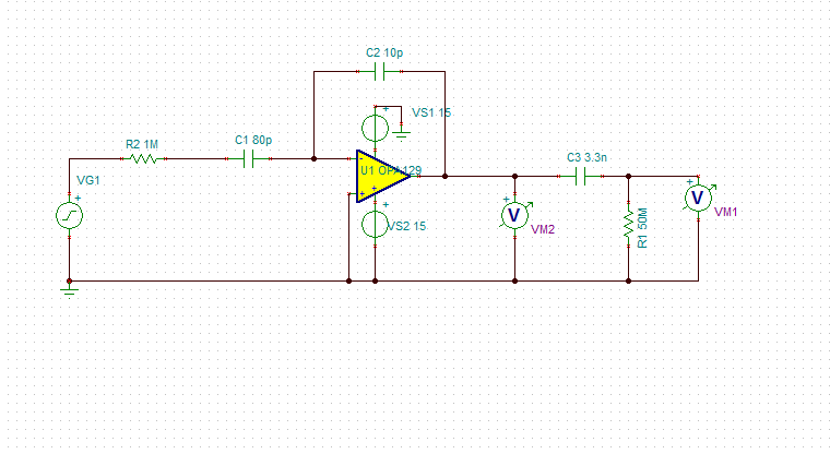
I am configuring the integrator and circuit diagram is attached. I don't have a background in electronic and I am just building circuit for my project. I am asking to expert to take have a look and help me to analyse the circuit and indicate any mistake. Additionally, I have another issue with gain of signal. Gain in this case C1/C2 but for some reason I am not able to see the gain practically. Any little help will do a job.
Kind Regards,
Zohra Malik
- - - Updated - - -
Here is attached circuit diagram:
I am configuring the integrator and circuit diagram is attached. I don't have a background in electronic and I am just building circuit for my project. I am asking to expert to take have a look and help me to analyse the circuit and indicate any mistake. Additionally, I have another issue with gain of signal. Gain in this case C1/C2 but for some reason I am not able to see the gain practically. Any little help will do a job.
Kind Regards,
Zohra Malik
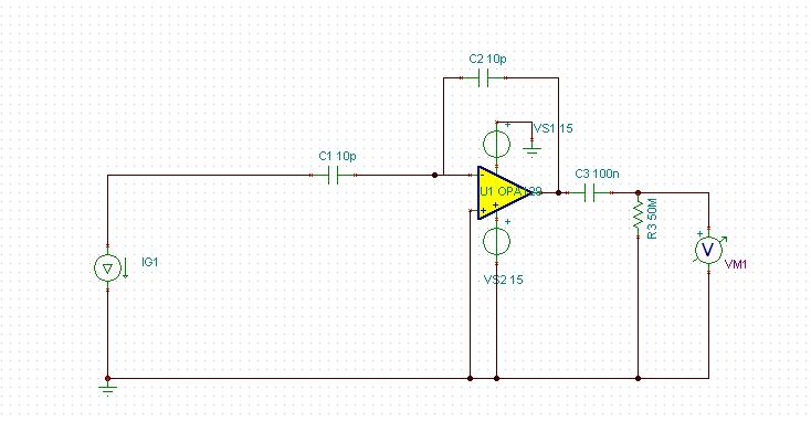
- - - Updated - - -
Here is attached circuit diagram: