Continue to Site

Welcome to EDAboard.com

Welcome to our site! EDAboard.com is an international Electronics Discussion Forum focused on EDA software, circuits, schematics, books, theory, papers, asic, pld, 8051, DSP, Network, RF, Analog Design, PCB, Service Manuals... and a whole lot more! To participate you need to register. Registration is free. Click here to register now.

help: bandgap reference with curvature-compenstation

Status
Not open for further replies.

turtlewang

Member level 2
Joined
Nov 7, 2010
Messages
46
Helped
1
Reputation
2
Reaction score
1
Trophy points
1,288
Activity points
1,605
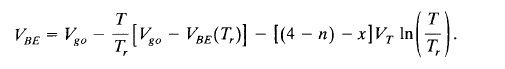
I have read the paper named A Novel Wide-Temperature-Range 3.9ppm/C CMOS bandgap Reference Circuit which is published on Feb. JSSCC2012.

The link of this paper is:
https://www.google.com/url?sa=t&rct...qZzECQ&usg=AFQjCNE75T-dmCLqHDwfHne6d6u0ivF1gw


But I don't know how does the equation(8) in the paper come from. I think there are only three terms in the equation.

I have emailed to the author, but without any response.

Can anybody help me understand it?
 

Hello turtlewang.

Equation (8) showed in this paper is correct. Sometimes you see the equation written in a different way, like below. It may be the reason of you doubt. Both are the same equations.


Regards,
 

Thanks Palmeiras,

I am so sorry that, I mean Equation (18) not the Equation (8).

So sorry!

I think there are only three terms in the equation. The term with R5 should not in the output current.


Hello turtlewang.

Equation (8) showed in this paper is correct. Sometimes you see the equation written in a different way, like below. It may be the reason of you doubt. Both are the same equations.


Regards,
 

Need help. Is there anybody can give me some suggestion?

Thanks
 

Hi, i guess you are right...the R5 terms shouldn't be there..it is the R4 which is supplying the Non-Linear current....seems to me that R5 is just trying to make the current through Q3,Q4 a bit more constant...
 

Thanks very much!

So the term R5 is do nothing to improve the temperature coefficients of the output voltage. Right?

Hi, i guess you are right...the R5 terms shouldn't be there..it is the R4 which is supplying the Non-Linear current....seems to me that R5 is just trying to make the current through Q3,Q4 a bit more constant...
 

May not be in a direct way....as per the theory, current into Q3,Q4 needs to be a constant current and without R5, it wont be constant exactly...there will be some nonlinearity, so i am guessing that R5 is just making sure that the current into Q3,Q4 is relatively more constant. So there might be improvement but could be very little. Without the R5 and Mp11, Mp12 branch the concept is the same as Malcovati's paper (except for the CTAT current generation)
 

Thanks very much!

I think the arrow direction of R5 is wrong. Since the current is following from Node E to Node D. Since the voltage at node A,B,C and E are the same as per the theory.

And another question is how to size Q3 and Q4? I think the ideal size is to make the current density of Q3 and Q4 equal to Q1 at the reference temperature Tr, which satisfying : size(Q3+Q4)/size(Q1)=(I_PTAT+I_CTAT)/I_PTAT.

But at the reference temperature, the current flowing through Q3 and Q4 is the sum of PTAT current and CTAT current which is not two times of the current following through Q1.

So I think the size of Q3 and Q4 are chosen randomly, because we can't get the accurate size. We need extensive fine tuning the resistor.

Is my understanding right?


May not be in a direct way....as per the theory, current into Q3,Q4 needs to be a constant current and without R5, it wont be constant exactly...there will be some nonlinearity, so i am guessing that R5 is just making sure that the current into Q3,Q4 is relatively more constant. So there might be improvement but could be very little. Without the R5 and Mp11, Mp12 branch the concept is the same as Malcovati's paper (except for the CTAT current generation)
 

Yes you are right..the Vbe0 values should be the same at node A(B) and node D..so any deviation will result as an offset (in this case it will be CTAT) which again has to be adjusted by tuning either or both of R2, R1
 

Thanks very much! I will read it again more carefully. Thanks again.
Yes you are right..the Vbe0 values should be the same at node A(B) and node D..so any deviation will result as an offset (in this case it will be CTAT) which again has to be adjusted by tuning either or both of R2, R1
 

Status
Not open for further replies.

Part and Inventory Search

Welcome to EDABoard.com

Sponsor

Back
Top