Continue to Site

Welcome to EDAboard.com

Welcome to our site! EDAboard.com is an international Electronics Discussion Forum focused on EDA software, circuits, schematics, books, theory, papers, asic, pld, 8051, DSP, Network, RF, Analog Design, PCB, Service Manuals... and a whole lot more! To participate you need to register. Registration is free. Click here to register now.

Help about this level shifter circuit

Status
Not open for further replies.

bhl777

Full Member level 6
Joined
Sep 30, 2008
Messages
363
Helped
0
Reputation
0
Reaction score
0
Trophy points
1,296
Activity points
5,140
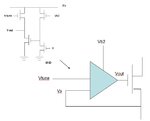
Hello everyone, I met a circuit configuration and want to understand how it works. It seems like Vtune has a linear relationship with Vx. Can anyone do some analysis for the attachment?
P.S: Do we need the outer circuit (the output of the triangle connects with the gate of another MOS) to analysis this shifter?
 

Attachments

  • 1.jpg
    1.jpg
    20.3 KB · Views: 180

This looks like a linear low dropout regulator (LDO). I'm assuming that all transistors are PMOS except the Vx input transistor that is NMOS and all in saturation. Vtune is a current source that will change the amount of voltage shift that Vout will have. The NMOS with input x is operating as a common source amplifier, then the PMOS will add a level shift of Vgs2 proportional to Vtune. Changing the current using Vtune will change the Vgs2, so the final Vout=Vx+Vtn1+Vgs2. The idea is to make the (Vgs-Vtn) of the big transistor as small as possible so you have a low dropout between its drain and source.

The outer circuit is just to show the loop used. Assuming the big transistor is a common drain NMOS , you will have an inversion in the loop due to the common source NMOS and since the level shifter has a gain ~1, you have a negative feedback loop. The idea is to make Vtune=Vx while adding high current capabilities at the load connected at Vx. The level shifter is needed since you want to make Vds=(Vout-Vx-Vtn), then adding the Vgs2, you make sure that the transistor is always operating in saturation for a reasonable amount of current and with a small Vds.
 
  • Like
Reactions: bhl777

    bhl777

    Points: 2
    Helpful Answer Positive Rating
Hello adriancm5, thank you very much! But I am a little bit confused of the numbers you mentioned of the transistor, could you use this picture to explain to me again? I assume you mean only M1 is NMOS while M2-M5 are PMOS, is it correct?
1.png
This looks like a linear low dropout regulator (LDO). I'm assuming that all transistors are PMOS except the Vx input transistor that is NMOS and all in saturation. Vtune is a current source that will change the amount of voltage shift that Vout will have. The NMOS with input x is operating as a common source amplifier, then the PMOS will add a level shift of Vgs2 proportional to Vtune. Changing the current using Vtune will change the Vgs2, so the final Vout=Vx+Vtn1+Vgs2. The idea is to make the (Vgs-Vtn) of the big transistor as small as possible so you have a low dropout between its drain and source.

The outer circuit is just to show the loop used. Assuming the big transistor is a common drain NMOS , you will have an inversion in the loop due to the common source NMOS and since the level shifter has a gain ~1, you have a negative feedback loop. The idea is to make Vtune=Vx while adding high current capabilities at the load connected at Vx. The level shifter is needed since you want to make Vds=(Vout-Vx-Vtn), then adding the Vgs2, you make sure that the transistor is always operating in saturation for a reasonable amount of current and with a small Vds.
 

Hello adriancm5,could you please tell me that from the picture in #3, are both M1 and M5 NMOS? I tried a few times to understand your explanation but feel very confused of the "big transistor" you mentioned because from somewhere it should be M1 and somewhere else it is M5. Please help me, thank you!

This looks like a linear low dropout regulator (LDO). I'm assuming that all transistors are PMOS except the Vx input transistor that is NMOS and all in saturation. Vtune is a current source that will change the amount of voltage shift that Vout will have. The NMOS with input x is operating as a common source amplifier, then the PMOS will add a level shift of Vgs2 proportional to Vtune. Changing the current using Vtune will change the Vgs2, so the final Vout=Vx+Vtn1+Vgs2. The idea is to make the (Vgs-Vtn) of the big transistor as small as possible so you have a low dropout between its drain and source.

The outer circuit is just to show the loop used. Assuming the big transistor is a common drain NMOS , you will have an inversion in the loop due to the common source NMOS and since the level shifter has a gain ~1, you have a negative feedback loop. The idea is to make Vtune=Vx while adding high current capabilities at the load connected at Vx. The level shifter is needed since you want to make Vds=(Vout-Vx-Vtn), then adding the Vgs2, you make sure that the transistor is always operating in saturation for a reasonable amount of current and with a small Vds.
 

yes, that was my asumption, but it depends on your final circuit. According to your picture, M1 is a common source NMOS transistor, M4 is a PMOS current source, M2 is a PMOS level shifter, M3 is a PMOS tunable current source and I'm assuming M5 will be an NMOS and that's why you will need a level shifter so you can make sure the transistor is always in saturation.

In order for the loop to be stable you need an even number of inversions so the M5 should be a source follower NMOS so you have only one inversion from the common source NMOS M1 so you have a negative feedback loop. I hope this is more explanatory.
 
  • Like
Reactions: bhl777

    bhl777

    Points: 2
    Helpful Answer Positive Rating
Status
Not open for further replies.

Similar threads

Part and Inventory Search

Welcome to EDABoard.com

Sponsor

Back
Top