givensoo
Newbie level 6
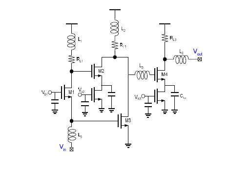
Now i am making a UWB lna, but if we put the Power supply PAD and the bonding wire Pad(of course include the bonding wire) on and simulate. the result is terribly bad.
the resone i guess is that : an inductor(bongding wire) connects to the source of the MOS, so it becomes a source degeneration structure.
But a lot of papers i read haven't mentioned this(i think it is a huge problem). so what can i do to steer clear of this trouble?
btw: the lna just has a single input not diff for the system's structure.