Continue to Site

Welcome to EDAboard.com

Welcome to our site! EDAboard.com is an international Electronics Discussion Forum focused on EDA software, circuits, schematics, books, theory, papers, asic, pld, 8051, DSP, Network, RF, Analog Design, PCB, Service Manuals... and a whole lot more! To participate you need to register. Registration is free. Click here to register now.

[SOLVED] Heavy ringing in gate drive output - IR2117

Status
Not open for further replies.

nenya

Newbie level 6
Joined
Jul 18, 2012
Messages
11
Helped
0
Reputation
0
Reaction score
0
Trophy points
1,281
Activity points
1,384
Hi,
I'm using the IR2117 driver for the high side MOSFET IRFP450. My switching frequency is 100 kHz and the application is in a buck converter circuit with an input supply of 10 V stepped down to 1 V. I followed the circuit given in the datasheet to test my gate driver. I'm sorry I'm unable to attach the typical connection circuit. I will give the link to the datasheet here.
http://www.irf.com/product-info/datasheets/data/ir2117.pdf

I used a 4.7 microfarad capacitor between Vcc and COM and a 1 microfarad capacitor between Vb and Vs.

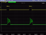
I'm giving the logic input to the driver from a function generator. I'm attaching the oscilloscope snapshot of the gate drive input (top trace) and the gate drive output (bottom trace). This is in the buck converter circuit.

Please help me understand why the massive ringing is happening during the switching, and what I can do to eliminate or reduce the severity of the problem. If I have not provided sufficient details please let me know so I can give more details of the circuit. Thanks in advance.


The heavy ringing happens only in the buck converter circuit. When I test only the gate driver circuit connected to just a MOFSET, there is no ringing effect.
 

Attachments

  • IR2117TypicalConnection.bmp
    1.5 MB · Views: 132
  • Gate output.png
    Gate output.png
    75 KB · Views: 161
Last edited:

Hi Nenya
and a 1 microfarad capacitor between Vb and Vs.
That capacitor is boot strap capacitor , and most important part of driver ( float drivers ) so , it's value seems a bit low , you can increase it's value up to 47 u or perhaps 100 u or a bit higher , thus i think the result will be better .
Best Wishes
Goldsmith

- - - Updated - - -

i.e : 1uf seems too low .
 

Bad measurement setup, more likely bad circuit layout. Rarely a problem of bootstrap capacitor dimensioning, rather bootstrap capacitor in the wrong place.

We'll want to see power output waveform together with the gate signal, and a photo of the full circuit to get an idea what's happening.
 
Hi Goldsmith and FvM,

Thank you very much for your timely replies. I'm new to hardware and prototyping. A lot of what little I have learnt so far has come from reading the discussions on edaboard. I appreciate your time in helping me.

Goldsmith, could you please explain the need for a larger capacitance? I used the formula for bootstrap capacitor requirement as given in the application note and got a figure in the nF scale. And I have used a uF level cap here. Could you elaborate on the theory if it's not too much trouble?
FvM, what is a bad measurement setup? Do you mean the settings in the oscilloscope? Do you have any material on a good circuit layout? I could do with some pointers.

I haven't been able to work on my circuit for a day now. I will post the circuit layout as well as the oscilloscope captures in a couple of days. I will be glad to receive your feedback once I do so. Apologies for the delay, once again.
Many thanks!
 

FvM, what is a bad measurement setup?
I meaned hardware setup, e.g. selecting probes, how to connect them, where to connect ground leads. "Bad measurement" is the little sister of "bad circuit layout", metaphorically speaking.
 

could you please explain the need for a larger capacitance? I used the formula for bootstrap capacitor requirement as given in the application note and got a figure in the nF scale. And I have used a uF level cap here. Could you elaborate on the theory if it's not too much trouble?
Hi Nenya
The reason for larger capacitor , is : most of the times leakage resistor , of each capacitor , is trouble maker ! your capacitor should be able to keep enough charge , and then should be able to handle high value of surge current . so , if it's capacity be higher , it can make higher , surge currents too .
Good luck
Goldsmith
 

Hi,
I'm uploading the image of the converter as well as the oscilloscope output. (Oscilloscope Trace 1: Logic input to the gate driver, Trace 2: Gate driver output, Trace 3: Drain-source voltage of MOSFET)buck.jpgbuck000.png
I'm using a 10 V to 1 V step down converter, with IR2117 as the high side driver for IRFP450 switching at 100 kHz. The inductor is a 330uH, 4.5A rating Murata inductor and the capacitor is a 680uF, 16V Rubycon.
Dear Goldsmith,
I tried using both a high as well as a low capacitor for the bootstrap. It did not provide a lessening effect in the ringing. I'm quite puzzled!
I hope I will be able to get some clarity on this problem. thank you once again, FvM and Goldsmith for your time and patience. Looking forward to receiving valuable inputs from you and others as well.
 

The photo clarifies everything. The problem is that the term breadboard isn't mentioned in your posts.

I fear, there's little chance to get better waveforms in a breadboard setup. You can try with a gate series resistor, e.g. 5 to 22 ohm, although it's supposed to increase switching losses.
 
Hi FvM!
thanks for your prompt response. since I'm new to prototyping, could you please explain why a breadboard would be a deciding factor (as in this case) for such a response?
Do you mean to say that the heavy ringing can be eliminated if I patched up this circuit on say a stripboard or a PCB? I thought a breadboard was suitable for usage up to a few MHz of switching frequencies?
 

In a short, the ringing is caused by the large circuit inductances of the breadboard setup. Stripboards can be better, but seem still problematic for 100 kHz switcher circuits.
 
Ah, okay I get it. Since a PCB might not be an easy or ready solution for test prototyping, what would you advice as a starting medium for high frequency circuits, if a breadboard cannot be used?
 

Hi Nenya
I came back again ! but i'm a bit surprised ! because i didn't expect that you did it on bread board ! as FvM said , the problem can be because of bread board . ( a bread board is a complete RLC circuit regarding high frequencies) . ( 100 KHZ isn't high but it is an square wave , hence other harmonics will be higher ! for high frequency circuits a good PCB will be required with polygon of GND and star ground . and don't forget that capacitors should be nearby inductors ( related capacitors ) and power node should be as near as possible to your switch . thus you won't have any problem .
Best Wishes
Goldsmith
 
Last edited:
Hi Goldsmith,
Thank you so much for the tip! I will remember this for future testing. I will also try rearranging the components to see if it makes a difference.
Thanks a lot for your time!
 

Just to post a quick update:
While doing the individual pin testing of the MOSFET, I noticed that there was heavy ringing only on the drain voltage and the source voltage. I placed a capacitor across the supply (Vin+ and Vin-) to the MOSFET and the ringing subsided by a significant margin. I expect it was the noise from the host voltage source which was a main culprit in the driver ringing.
Hi Nenya
It means it was because of equivalent circuit of your lines !
All the best
Goldsmith
 

Status
Not open for further replies.

Part and Inventory Search

Welcome to EDABoard.com

Sponsor

Back
Top