Continue to Site

Welcome to EDAboard.com

Welcome to our site! EDAboard.com is an international Electronics Discussion Forum focused on EDA software, circuits, schematics, books, theory, papers, asic, pld, 8051, DSP, Network, RF, Analog Design, PCB, Service Manuals... and a whole lot more! To participate you need to register. Registration is free. Click here to register now.

H bridge Switching Voltage Problem

Status
Not open for further replies.

Dale Gregg

Junior Member level 3
Joined
Jul 23, 2013
Messages
29
Helped
2
Reputation
4
Reaction score
2
Trophy points
3
Location
Leeds, United Kingdom
Activity points
263
CICnoLC.PNG
Hi, I'm simulating my inverter but finding a efficiency of 35% across the switching circuit. I calculated the switching voltage as 35V but this produces a Vpeak of 18.5V and 65A at the output.

I bypassed the filter and connected the oscilloscope as shown above and this is the output,
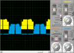
Vsw35.noLC.PNG

The peak pulses are at about 20V and then either side there a drop. The positive cycle starts at the same level and then drifts upward as shown.

I adjusted the switching voltage down to 20V,
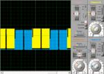
Vsw20.noLC.PNG

This gives a much clearer 28V pulse which was my target peak voltage.

Could any one help me under stand why this is happening?
The carrier frequency is 15.6KHz, driver voltage is 23V, target current is 100A on to a 200mΩ load.

Vsw=Psw/Isw
Psw=Po/eff
Po=Vp*Io (peak)
Vp=(Io*Ro)/0.707107
Vp=(100*0.2)/0.707107=28.28 (max DC=0.98) 28.28/0.98=28.86
Po=100*28.86=2886
Psw=2886/0.82=3520
Vsw=3520/100=35.20V

Have I made a mistake here, as Im getting my target results from 20V? Any help would be great.
Regards,

Dale
 
Last edited:
Not sure I'm looking at this right, but do you have the sources on the bottom of your bridge connected to -35V? If so, you'll never EVER turn off those bottom MOSFETs.
 
Ye but I found in the simulation that if I dont use bipolar and tie to ground instead I get something like this,
**broken link removed**

Thats at 4MHz clock with filter, if I try at 16MHz I just get groups of pulses about 1uS long? Any Ideas how I can round this??

- - - Updated - - -

I think its to do with the driver circuit,
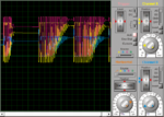
unipole.Vsw35.16mhz.PNG

Channel A yellow is the output through the filter, Channel B Blue is the High side output from the driver, and C purple is the low side and this is at 10uS/D. so the problems coming from the driver. Is there anything obvious I've missed in the driver circuit?
 

You are applying 300 kHz gate pulses? That's far beyond feasible circuit speed.

You are also exceeding Vgs and Vds rating of the transistors. This must not necessarily matter in simulation but can't work in a real circuit.

As mentioned by barry, driver ground must be tied to negative bus voltage.
 
Hi thanks, The switching frequency in the last image is 15.6KHz. I've changed the circuit so that ground is connected to the source's of the low side switches and rolled back the switching freq to 3.9KHz (4MHz clock).
I'm getting the target results, 0-100A but the waveform is a bit deformed....
unipoleVsw35.PNG

What could be effecting this?

Regards,

Dale
 

Which load is used in simulation?

A general problem of your design is that is apparently not using synchronous switching. As a result, an output voltage according to the pwm duty cycle can be achieved for pure resistive loads, but not with reactive loads, e.g. a sine filter.
 

New.PNG

Hi, this is the circuit as it is now. RL of value 0.2 is the load with a LC filter before it on the output of the bridge. I thought this was a synchronous design? Q1 and Q4 switch the pulse train whilst Q2 and Q3 are off then they switch the signal whilst Q1 and Q4 are off or have I got the wrong idea?

In real life would I need transformer isolation before the LC filter too?

Thanks,

Dale
 

Q1 and Q4 switch the pulse train whilst Q2 and Q3 are off then they switch the signal whilst Q1 and Q4 are off
This isn't synchronous switching. It would involve complementary activation of Q1/Q2 and Q3/Q4 (with a small deadtime inbetween).

Synchronous switching in a H-bridge can be implemented either in a 2-level or 3-level scheme. The latter needs 4 independent controllable PWM outputs (or 6 fof it for a three phase bridge) which aren't available in small PIC processors.
 
Last edited:
Hi,
I am trying to do the same project, however it's not clear to me why and how the voltage is 170 V on the output. The researches I found did not explain what happens exactly in each circuit.
I would like to know why we need sine and triangle waves, what the pwm and h-bridge do and etc...

Thanks

dc ac.png
 

Status
Not open for further replies.

Similar threads

Part and Inventory Search

Welcome to EDABoard.com

Sponsor

Back
Top