Continue to Site

Welcome to EDAboard.com

Welcome to our site! EDAboard.com is an international Electronics Discussion Forum focused on EDA software, circuits, schematics, books, theory, papers, asic, pld, 8051, DSP, Network, RF, Analog Design, PCB, Service Manuals... and a whole lot more! To participate you need to register. Registration is free. Click here to register now.

H-Bridge power supply shorting

Status
Not open for further replies.

nadre25

Member level 3
Joined
May 15, 2009
Messages
56
Helped
0
Reputation
0
Reaction score
0
Trophy points
1,286
Activity points
1,780
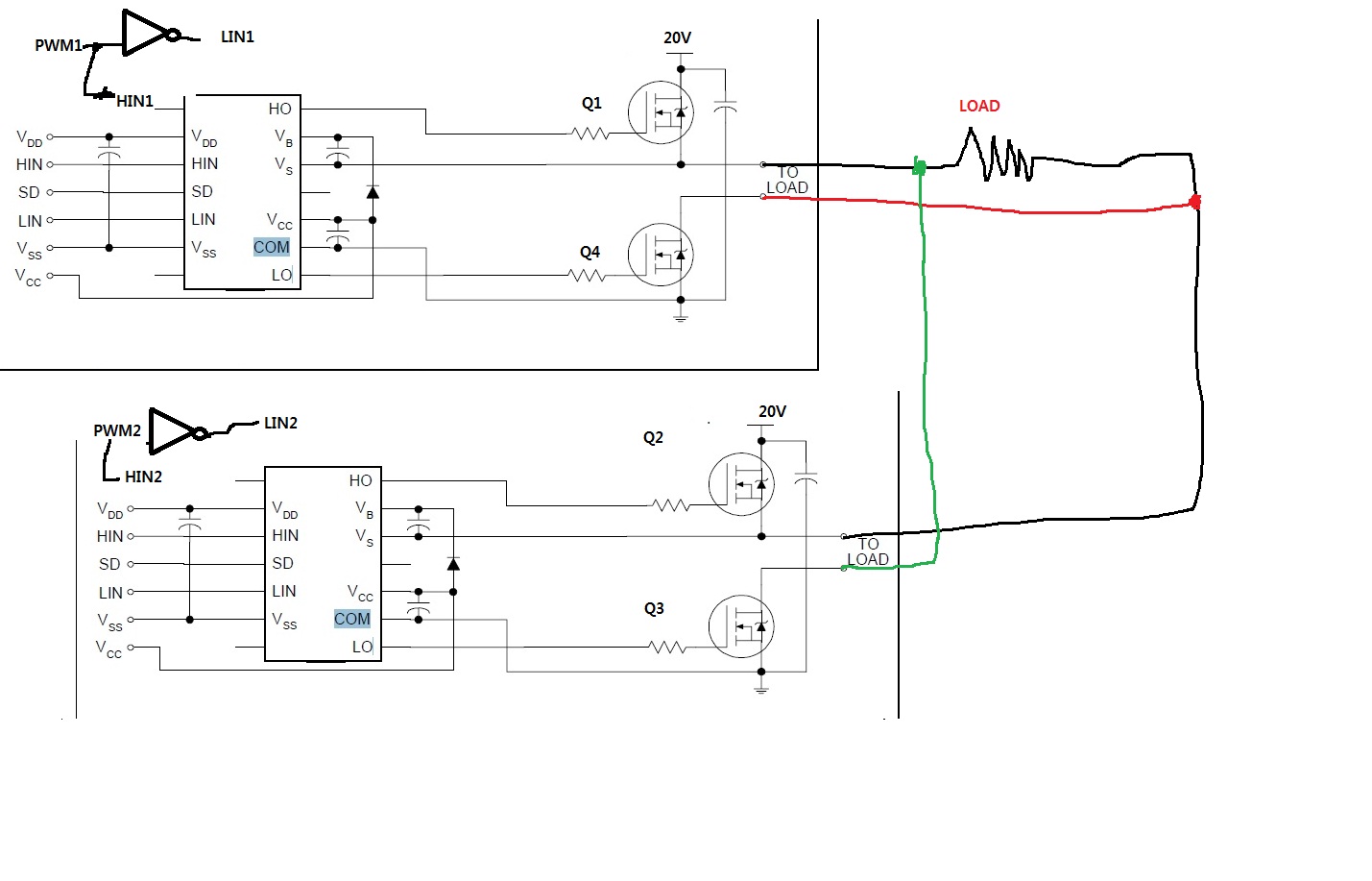
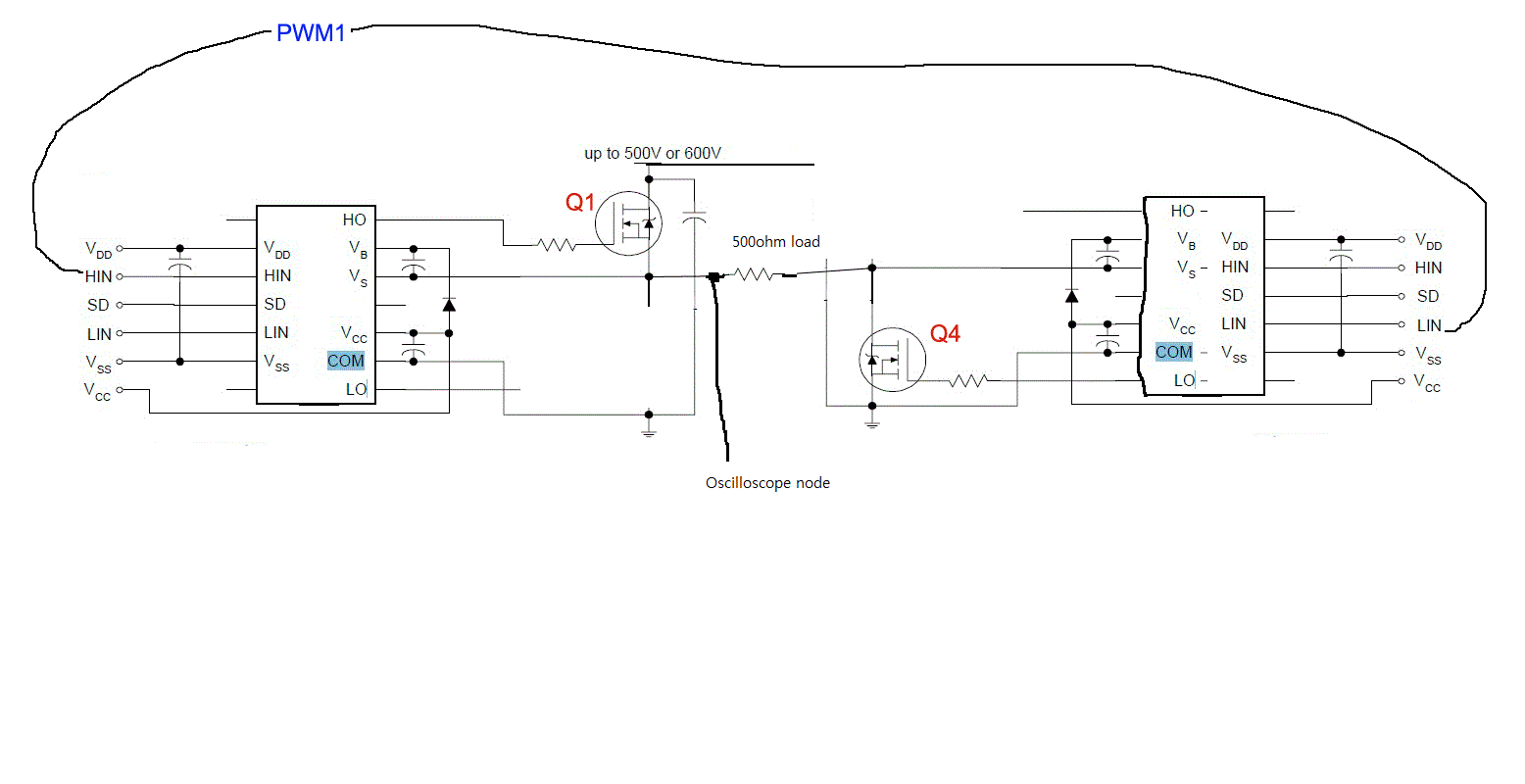
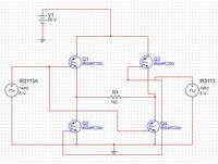
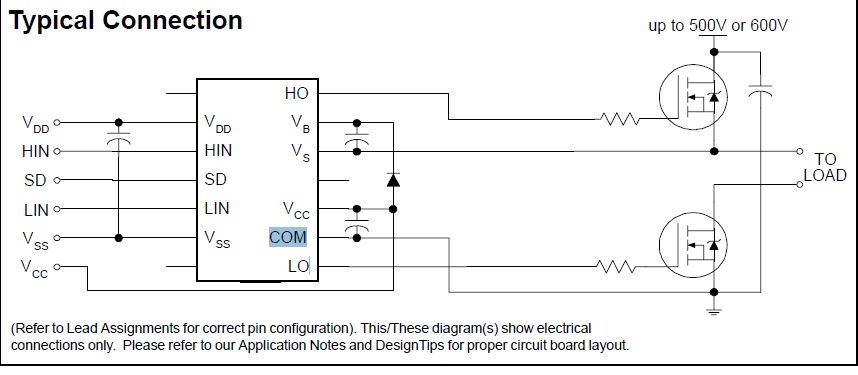
Hi we are having a problem with our H-Bridge. We used an IGBT and IR2113 as its gate driver. We already saw another post but for some reason we can't comment on it... so we made a new one.

Our Voltage Input on the H-Bridge is 20V
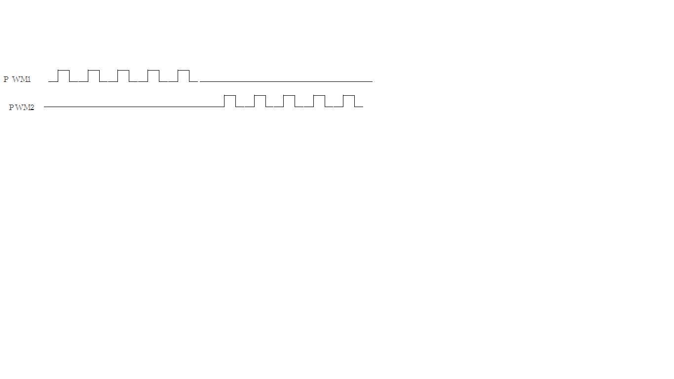
The signal voltage source just represents our input on the gates, its PWM driven. the PWM comes from our microcontroller, we programmed it in such a way that at a certain time ONE pair of IGBT'S are ON and the other pair is OFF

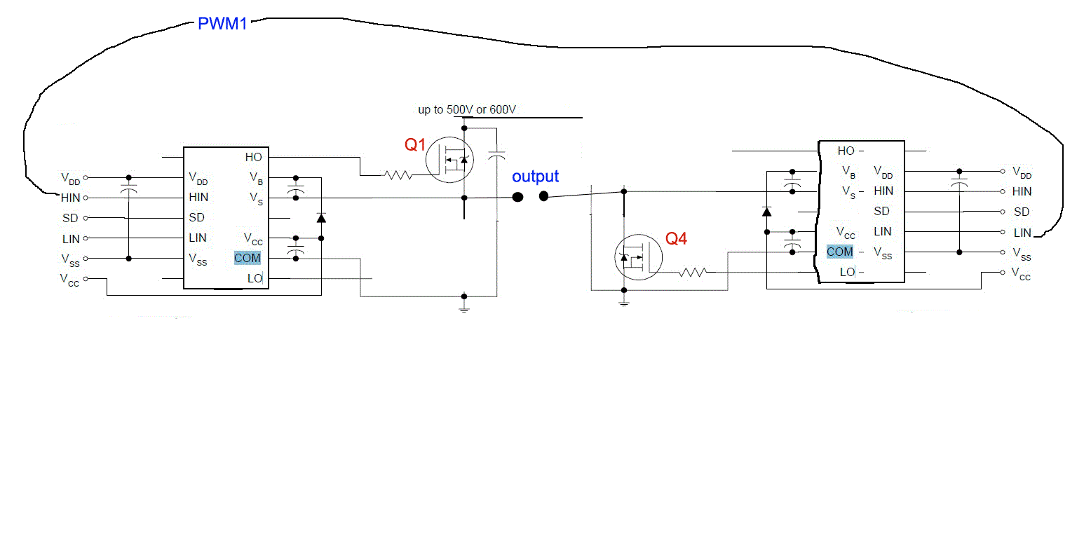
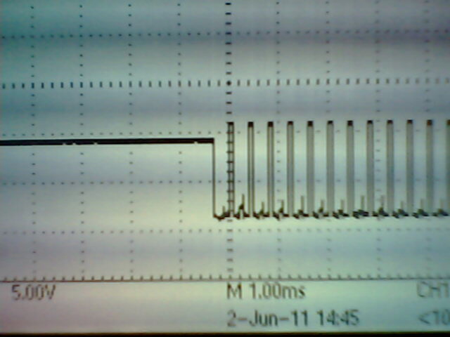
Problem: The 20V source is shorting once we connect it to the circuit. Q1 and Q4 are the transistors that turns on at the same time. and Q2 and Q3 are the other pair.

When we test it as a Half bridge by using Q1 and Q4 we get our desired output which is a square wave and same when using Q2 and Q3 only.

We really plan to use this on a motor to control it but for testing we are just using a resistor.

Are we lacking something?
Comments are appreciated. Thank You


post somewhat not clear .
whether the shorting is observed in real test or in simulation.

whatever it is , you have to add some deadtime in pwm pulse applied to igbt to avoid short(in realtime/simulation)
 

We added a deadtime. it is about 500miliseconds. We tried it in real time. Our power supply 20V is shorting.

Here is the image of our IGBT driver.

instead of a very high voltage, we are just using 20V

Vdd, Vcc = 12V

HIN = 10 - 12V pwm

LIN = 10 - 12V pwm we inverted this input is that correct???


You are using two IR2113 , the mosfets should be activated in pairs diagonally , Q1-Q4 or Q2-Q3.
Inverting the LIN (compared to HIN) would not be a problem but if both are driven from the same source then how can you add the deadtime?
Also note that you shouldn't invert the same input in both chips, you want to have HIN1 LIN2 active at the same time and then LIN1 HIN2.
HIN1 and HIN2 shouldn't be active at the same time, if they are driven by the same PWM one of them has to be inverted, the same thing applies to LIN1 LIN2.

Alex
 

but if both are driven from the same source then how can you add the deadtime?
Alex
Thanks for your reply,

Does the inverting of LIN and HIN have an effect on the deadtime?

from our understanding deadtime is when our output is zero. is that right? We just make the pwm input dutycycle for that pair of transistors down to 0.

We have another question, when you say "Also note that you shouldn't invert the same input in both chips" are you saying HIN1 and LIN1 should have same input and one should not be inverted? (HIN1 and LIN1 are in the same IR2113 which is driving Q1 and Q4)

We are using 2 PWM outputs by the way. We made them out of phase from one another through delays.

Thanks!
 

Does the inverting of LIN and HIN have an effect on the deadtime?

You can turn any input on with a positive voltage, if you feed a common PWM to two inputs and one of them is inverted then in either case one of them will be on , you cant turn off both of them.
Maybe I didn't understand exactly what you are doing, you have two PWM lets say PWM1 and PWM2 and you have HIN1 LIN1 HIN2 LIN2 , how are the PWMs connected to the inputs and where do you have the invert?

We have another question, when you say "Also note that you shouldn't invert the same input in both chips" are you saying HIN1 and LIN1 should have same input and one should not be inverted? (HIN1 and LIN1 are in the same IR2113 which is driving Q1 and Q4)

I meant that HIN1 and HIN2 or LIN1 and LIN2 shouldn't have the same input.
I have assumed that each chip was driving the left or right side, one chip to Q1-Q2 and the other Q3-Q4, I haven't seen an IR2113 drive diagonal mosfets, maybe it can be done but why don't you follow the typical application schematic?

Alex
 
Last edited:

I would be better, if you show a complete schematic of your setup, including power supply sources and their ground connection. Up to now I saw a completely absurd schematic in post #1, that shorted the gates of high side and low side drivers crosswise. And a copy from the IR2113 datasheet in post #3. So what's your real circuit?

In addition, if you say, the supply is shorted, did you check the IGBTs for possible internal shorts?
 

Hi FvM and alexan_e. i just edited my post #3 this is exactly what we assembled. the top IR2113 drives Q1 and Q4, LIN1 is inverted but it came from same PWM source as HIN1. same explanation from the bottom IR2113 which drives Q2 and Q3.

for testing, we only used 20V supply, the problem we are having is that when we turn everything on, this supply starts to SHORT. However if it is only a half bridge, like if we remove Q2 and Q3. The circuit works.

All of them have same grounding, supply, inverter, microcontroller where we get our PWM and IR2113 all have the same ground. We have also tried checking the IGBTS their all working :)


It is imperitive that only one pair is conducting at any time. Even a very short overlap, during which both pairs conduct, will put a short across the supply.

Once Q1 and 4 stop conducting, there should be a small wait until Q2 and 3 start to conduct, and vice versa. As far as I can see from the diagram, there is no such waiting time.

Pertaps what is being referred to as the "dead time" means the same thing, but I can't see it built in.
 

Hi Syncopator, How do you suggest do we solve the problem of deadtime? is it in the programming of the microcontroller or is it a circuit?
Thanks!
 

I think it's almost certainly the program. The drive to one pair needs to be inverted and delayed, and the subsequent drive to the first pair delayed too, etc.
 

The present control signal wiring in fact doesn't allow a software programmable dead time. It would be possible for a bipolar PWM scheme (left and right halfbridge switching simultaneously to the opposite level) with a different wiring, omitting the inverters. Phase A is fed to HIN1 (left) and LIN2 (right), Phase B to HIN2 (right) and LIN1 (left). Both phases are activated concurrently with short deadtime (both outputs low).
 

There is no way to add dead time when you use inverters, to use deadtime you have to have off all four inputs (HIN1, HIN2, LIN1, LIN2) but because of the inverter two of them are always on.
I would suggest something like this

IR2113.gif

Alex
 
  • Like
Reactions: kurtee

    kurtee

    Points: 2
    Helpful Answer Positive Rating
this is the program that we used for our circuit. attached is the waveform of the code.

while(1){
Pwm1_Change_Duty(150);
Pwm2_Change_Duty(0);
Delay_ms( 8 );
Pwm1_Change_Duty(0);
Pwm2_Change_Duty(0);
Delay_ms(500);
Pwm1_Change_Duty(0);
Pwm2_Change_Duty(150);
Delay_ms( 8 );
Pwm1_Change_Duty(0);
Pwm2_Change_Duty(0);
Delay_ms(500);
};


basically, what were trying to do is, turn on one pair of igbt then turn it off then turn on the other pair of the igbt.

do you think it might be the inverters fault because if it would always be logic high if our output from the microcontroller is 0?
 
Last edited:

Yes, as I wrote in the previous post you can't turn off everything using the inverters.
Your pwm pulses have a dedtime but it can't be applied unless you remove the inverters.
Use a circuit like the one I have posted.

Alex
 

We tried the circuit that you posted, but only tried it on a half birdge circuit first. This is what we did


This is what we saw from the output waveform taken on the load, we just used a 12V to 13V DC supply this time connected on the drain of the highside IGBT. The square wave is a little distorted due to the setting of the oscilloscope but what we noticed is that there is still a DC Voltage on the left side of the image. Shouldn't the reading on that left side be 0V? Based on the PWM we are using from our previous post, the dead time we used, there is a point where the pwm is 0V so both igbts should be off and no voltage would go across the load. At the time where the square waves are present, that is the time when our IGBTS are turning on and off at the same time.


So you say that you have 9v at the output when the inputs are off (low)?
Did you have a load connected or is the output floating?
I'm not sure about the correct operation of the circuit without the low side switch because the charging of the bootstrap capacitor is based on the existence of that low side switch that is on when the high side is off.
I don't see a way to charge the bootstrap capacitor with the schematic you have presented.

Alex
 

Please show both PWM input waveforms to make understandable what you are doing.

P.S.: If precharging of the bootstrap capacitors is an issue, it can be achieved by activating both low side drivers simulataneously in a first step. Unfortunately individual control of all 4 switches or additional logic is required to achieve this.

But due to the undervoltage lockout feature of IR2113, it isn't a problem in most cases. After the first full output cycle, the bootstrap capacitors should be charged completely. The output duty cycle of this first cycle is however uncertain. So if you are required keep the DC balance strictly, a precharge means should be considered.

But I don't expect, that your observations are related to precharge problems.
 
Last edited:

Use the full bridge to test the operation, if the pwm are correct you will have no problem.
If you are afraid that you might get a short use a psu with a current limit for the IGBT supply or use a resistor (say 5 ohm) and feed the positive supply to the IGBT through it so that it can limit the current to 2A if something goes wrong.
The load should have higher resistance than that resistor like for example 100ohm.

Alex
 

The output that we have as seen in the picture is approximately 10 to 12V. From the wave, we believe the time or point in the oscillosope where there is a squarewave is the time where the PWM turning on and off (switching). And the straight line voltage on the left side of the image is our dead time. we dont know why there is a voltage there when it should be 0V.

The PWM input that we used is this


we only used PWM1 for the test

Our load was a resistor, 500ohms. it was connected from the source of the Highside IGBT to the drain of lowside igbt.


when you say the low side switch, is it the low side switch on the same side of the highside IGBT or do you mean the lowside pair of the highside igbt?
 

Status
Not open for further replies.

Similar threads

Part and Inventory Search

Welcome to EDABoard.com

Sponsor

Back
Top