Continue to Site

Welcome to EDAboard.com

Welcome to our site! EDAboard.com is an international Electronics Discussion Forum focused on EDA software, circuits, schematics, books, theory, papers, asic, pld, 8051, DSP, Network, RF, Analog Design, PCB, Service Manuals... and a whole lot more! To participate you need to register. Registration is free. Click here to register now.

h bridge heating problems

Status
Not open for further replies.

ian123

Junior Member level 3
Joined
Aug 26, 2011
Messages
31
Helped
3
Reputation
6
Reaction score
3
Trophy points
1,288
Activity points
1,510
hi

i have designed a mosfet hbridge but am having heating problems please could you help with this.

the hbridge consists of rectified mains voltage with 330 uf 400v cap on the high side the polarity is being switched every two seconds.
the lo side is on for 2 sec and the high side is being pwm at 94hz for the two secs then switched off and the other side is switched on.
the load does not go over 3 amps.

i have two problems the bridge rectifier gets hot (8Amp 600v). the mosfets get hot after a while.

the load is passive but the current changes all the time.I am inserting two probes into a gel which will warm up over time.

the mosfets are on small heatsinks due to my reasoning that they are no where near their limit.
 

How are you driving yours mosfets?
gate drivers?
 

Upload the circuit schematic for better response and help.
 

Here is the schematic
 

Attachments

  • Polarity Switching device V5.pdf
    22.6 KB · Views: 150

please provide me with some info

if a load is drawing 3 amps at 300v then p=I x v therefor 3 X 300 = 900 watts

does this mean that 900watts is the heat in the mosfets and the mosfets have to be able to sink this heat

or does the load take this 900 watts

if the mosfets take this it would explain why they are getting hot. if this is the case would parralleing the mosfets up solve the problem or should i look at something else.

also in the spec sheet for the irfp460 it states the mosfet as having VDs of 500v and Id of 20A 80A if pulsed howcan that be if the max wattage is 280 watts

ie: 500 x 20 = 10 000 watts not 280

please explain
 

the hbridge consists of rectified mains voltage with 330 uf 400v cap on the high side the polarity is being switched every two seconds.
the lo side is on for 2 sec and the high side is being pwm at 94hz for the two secs then switched off and the other side is switched on.
the load does not go over 3 amps.
You're going to have to explain your switching operation a lot more clearly... you say the lo side is on while the high side is pwm'ed. I assume you're talking about transistors on opposite half bridges... I'm not sure why you even need an H bridge, especially at such low frequencies.

Also when using those bootstrap ICs, you need to be careful with low frequencies or discontinuous operation. Whenever you start using them after a period of non-use, you must turn the low side switch on first, in order to charge the bootstrap capacitor. If you don't do that then you will probably lose your gate drive voltage and that could easily explain the heating.
 

You're going to have to explain your switching operation a lot more clearly... you say the lo side is on while the high side is pwm'ed. I assume you're talking about transistors on opposite half bridges... I'm not sure why you even need an H bridge, especially at such low frequencies.

yes i switch opposite sides of the bridge on ie: hi one side lo otherside i require to switch polarity every two secs

Also when using those bootstrap ICs, you need to be careful with low frequencies or discontinuous operation. Whenever you start using them after a period of non-use, you must turn the low side switch on first, in order to charge the bootstrap capacitor. If you don't do that then you will probably lose your gate drive voltage and that could easily explain the heating.

i do turn the low side on to charge the caps for 10msec before turning on the hi side.

the circuit actually works but one the rectifier for the 300 vdc heats up and two the mosfets heat up.

please check my previuos reply and tell me your thoughts
 

please provide me with some info

if a load is drawing 3 amps at 300v then p=I x v therefor 3 X 300 = 900 watts

does this mean that 900watts is the heat in the mosfets and the mosfets have to be able to sink this heat
That is the power being delivered from the supply. Which components dissipate that power depends on their instantaneous current and voltage. If operated correctly, your H bridge should switch mosfets in a way such that they will never see high voltage and high current at the same time (thus they will dissipate little power always). Only the load should see both high voltage and high current simultaneously.
also in the spec sheet for the irfp460 it states the mosfet as having VDs of 500v and Id of 20A 80A if pulsed howcan that be if the max wattage is 280 watts

ie: 500 x 20 = 10 000 watts not 280

please explain
The max Vds means that's the maximum voltage that can be applied before breakdown occurs in the off state (not on state). The current rating is given in the on state. The device is not meant to be used with high voltage and high current simultaneously. When in the on state it can have large currents through it, but it should have low voltage across its terminals (like a volt or so). When it is in the off state it should experience high voltage (your supply voltage) but block all current flowing through it (microamps).
 

A 8A rectifier bridge without heatsink will run pretty hot at 3A.

For the transistor dissipation, these contributions have to be considered:
- conduction losses Pd = Id²*rdson*duty cycle, should be about 1 W per transistor at 3 A load current
- switching losses according to swichting, can be effectively neglected fo 100 Hz operation
- excessive losses due to overlapping gate voltages respectively insufficient dead time. Shouldn't be a problem with uC control, with reasonable gate voltage sequence
 

View attachment TIMMING.pdf
here is my new timming chart please advise if this is ok regards dead time

I have increased the duty cycle for hi side to 1.11mS and the period to 300 Hz
I have increased the Lo side duty cycle to 2.22ms and the period is 300 Hz

you will notice that the time between switching from forward to reverse is 4 usecs is this the dead time??

please explain the equation

PD= power dissipation
Id²= current drain does this equal 3amps²
Rdon= .27 ohms
Duty cycle = percentage or time = 25% or 1.11mSecs
 
Last edited:

Your rectifier is going to dissipate close to 2W (.6V forward drop x 3A) I think there's also a 1.4 time multiplier for bridges, I can't remember where that's from.

You should check the gate drive rise time. You want it to go from 0 to max as fast as possible so the MOSFET doesn't linger in the linear region. As the MOSFET transitions from full off to full on, there's a point where it's INSTANTANEOUS power is 450 W; you need to keep that time as small as possible to minimize AVERAGE power.
 

do i need to check the rise time with the 300v on or can i check it without the voltage on

if i check it with the voltage off then i have a perfect square wave on the gate

I dont want to check it with pwer on at the moment until someone explains the dead time.
is it the time from switching from one side if the h- bridge to the other or is it from the time the lo side 2 and the high side 1 switch off

---------- Post added at 22:52 ---------- Previous post was at 22:43 ----------

ok dead time is the time the between the hi side 1 and the lo side 2 switch on this is ok
 

The gate waveforms will definitely change depending on whether you apply power and a load, so test it with both, like in normal operation.

And yes dead time is between FETs on the same half bridge. At your frequency you should have at least a few hundred nanoseconds of dead time where neither FET is on.
 

Dead time isn't a problem with your drive waveforms. The problem is only arising, when you are switching between high and low side of one half bridge directly, but you don't.

The bridge rectifier power dissipation will be in fact twice the value of a single diode. According to a 8A datasheet that I have (KBU8), it's 2*3A*0.9V = 5.4W, resulting in about 100 K temperature rise with 18 K/W thermal resistance.

Switching times will be in a 100 ns range with the present driver circuit, that's why I said, switching losses are neglectable in this case. The verbose comments in this regard are valuable in general, but don't apply here.
 

i have a perfect square wave on the gate
No you don't.

Zoom in on your rising edge. You're charging about .004uF on that gate which takes a fair amount of current. At your low PWM rate (that is 94Hz, right not 94Khz?) it is probably ok.
 

ok only when swtching on the 300 vdc do i see the rising edge
 
Last edited:

please help me to understand some theory about power dissipation

I have a circuit as per above thread this circuit is for a passive load 3Amps @300vdc the power dissipated in the circuit is therefore equals P=I x V = 3 x 300=900 watts

I have read on the internet that to calculate the power dissipation of irpf406 mosfets P=I² x Rdson = 3²Amps x 0.027 = 2.43 watts
the mosfets are rated at max 280 watts.

therefore does 2.43 watts get disspated by the mosfets or does 900 watts get dissipated by the mosfets.

Also I need to then find a heatsink to sink the 900 watts if thats what it is .now the next question is

the max power dissipation of the irfp460 is 280 watts since there is two mosfets in each circuit means 280 watts x 2 ? = 560 watts

therfore 900 watts-560 watts = 340 watts i need to disspated by a heatsink. obviously one would like to derate the 280 watts to say 80 watts.

therefore 160 watts for the 2 ; 160watts - 900 watts = 740 watts i need to disspate by a heatsink.

if i need a heatsink to disspate 740 watts it would be a big heatsink in the order of a couple of meters since the heatsinks that i can get are 200 degrees per watt per meter lenght

Is my reasoning correct or am I missing the point. Obviously if its only 2.43 watts then the heatsink is smaller, but then why is my mosfets getting so hot.

i have the timming pdf in my previuos threads so one can see the timming for the switching on of the mosfets.

Please help thanks in advance
 

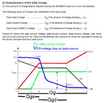
The power that is dissipated on a device (assuming resistive behavior) is I²*R so for the mosfet it is 2.43W as your calculation (assuming that you are correct on the RDSon) but note that this is the case only when the mosfet is turned on and stays in that state.
While you are in the switching state the dissipation is much higher and that is why we want to reduce that time as much as possible and we use high current drivers.

The steps involved when turning on/off a mosfet are shown in the graph below
Mosfer_gate_charge.jpg

The graph is from https://www.fairchildsemi.com/an/AN/AN-9010.pdf
see page 17 for the different gate capacitance charge stages.

The calculation of the dissipation in the switching state is king of complicated and I can't really help on that but it will be very short in duration since you are using a proper high current driver..
 
Last edited:

The 2.43 W calculation is basically correct. There are also other kinds of transistor losses involved, see my post #10.

The 280 W maximum rating is a more theoretical value, that won't be achievable in most cases, e.g. because you can't provide a respective heatsink size.
 

Status
Not open for further replies.

Similar threads

Part and Inventory Search

Welcome to EDABoard.com

Sponsor

Back
Top