Continue to Site

Welcome to EDAboard.com

Welcome to our site! EDAboard.com is an international Electronics Discussion Forum focused on EDA software, circuits, schematics, books, theory, papers, asic, pld, 8051, DSP, Network, RF, Analog Design, PCB, Service Manuals... and a whole lot more! To participate you need to register. Registration is free. Click here to register now.

guidance on the operation of the circuit -AM Receiver

Status
Not open for further replies.

the_falcon

Member level 4
Joined
May 28, 2010
Messages
72
Helped
0
Reputation
0
Reaction score
0
Trophy points
1,286
Location
Toronto
Activity points
1,811
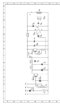
Can anyone explain and try helping me to understand this circuit operation. The transistor Q1 in the picture seems to work as a Colpitt oscillator, an envelope detector and also as a compensator for better selectivity of the resonant circuit. But I just dont understand that.
 

Attachments

  • AM_RR.png
    AM_RR.png
    78.3 KB · Views: 88
Last edited:

T1 is none of those.

It is simply a detector. The transistor's base-collector junction and base-emitter junction work like diodes and because the conduction varies slightly, the signal can be picked off the emitter. It isn't a good configuration because the transistor cannot work as an amplifier and the impedance across the tuned circuit is quite low which reduces it's 'Q' factor. I wouldn't expect it to work much better than if the transistor was replaced by a Schottky or germanium diode.

Brian.
 

Brian, Thanks but the user manual clearly says that the BJT T1 works as a colpitt oscillator, demodulator and also as a compensator to improve Q factor..I will paste the short description given for this circuit, along with this message..

A simple detector straight receiver consists of a oscillating circuit and a rectifier diode. The reception power is however limited, which means that only powerful stations can be received. The selectivity is also low, because both the antenna and the rectifier diode dampen the oscillating circuit, resulting in a large bandwidth. An Audion avoids these disadvantages and ensures very good sensitivity and selectivity.
The Audion transistor T1 has three functions: Amplification, compensation of the oscillating circuit and demodulation of the RF signal. The PNP transistor works as an emitter-follower. C2 and the internal base-emitter-capacitance of approx. 5pF form a capacitive voltage divider. A Colpitts oscillator is formed together with the oscillating circuit. The amplification can be chosen by suitably adjusting the emitter current, so the oscillator does not yet oscillate. At this operating point, the transistor adjusts all losses that occur in the oscillating circuit. The quality factor can be increased from about 50 to over 1,000. At a reception frequency of 6 MHz, the bandwidth is approx. 6kHz, it is thus possible to separate channels, which are close together.
The compensation also leads to an increase in signal amplitude. RF voltages of up to approx. 100 mV can occur at the base. The AM signals are demodulated to the input curve characteristic of the transistor. The NF signal then appears at the emitter. R1 and C2 form a low pass filter, which removes RF splits. T2 is an AF preamplifier for the integrated amplifier IC1. The AF stage also uses a PNP transistor to prevent any confusion when installing.
A special feature of the Audion circuit is the direct coupling of the transistor to the oscillating circuit. T1 operates with a collector emitter voltage of only approx. 0.6 v. In addition, the base emitter capacitance of approx. 5 pF has strong effects on the oscillating circuit. The close coupling ensures that the transistor also acts as a varactor diode and allows the fine tuning of the frequency via the feedback controller. Since the feedback applies very smoothly, you can attenuate a frequency of several kHz, which is advantageous for the reception of SSB and CW stations.
The loudspeaker amplifier LM386 works directly on a 9 V battery. The current consumption is very dependent on the set volume. At low volume, the entire receiver only draws approx. 5 mA. The LED not only serves as an on/off indicator, but also simultaneously to stabilise the LED forward voltage of approx. 1.8 V. The two transistors stages, therefore, will always receive a stable operating voltage.
 

I'm not going to get dragged into an argument over this but I still say it will not work very well. I'm not saying it won't work at all. There are other circuit configurations which are only slightly more complicated that will give significantly better performance.

Brian.
 

Thanks Brian for the information though
I just wanted to get cleared about this and thats why I was asking people here about it.
I dont see any oscillator working here though they explicitly told so, in the user manual

Thanks for your guidance.

Santom
 

I agree with Brian - I am not convinced it would work. It lacks the required feedback between the base and emitter. Relying on the internal base-emitter capacitance seems very dubious. Look at any Colpitts oscillator and you will see some pretty big capacitors providing the base-emitter feedback & phase shift. This has none. Just because a circuit "appears" to work doesn't mean it works for the right reasons. It could simply "work" because T1 is a rectifier, nothing else. You could always built it and see.

Keith.

---------- Post added at 14:25 ---------- Previous post was at 14:22 ----------

Just to add - it makes you wonder if C2 was supposed to go from base to emitter, not emitter to ground.
 

thanks keith for your opinion
the circuit works well like you assumed
 

Status
Not open for further replies.

Part and Inventory Search

Welcome to EDABoard.com

Sponsor

Back
Top