andres.m
Newbie
Hi guys,
I have been googling for a while and found lots of generic advice. However, I am struggling to narrow all down to my specific case. I know this is a complicated topic, but any help would be greatly appreciated.
In the attached schematic:
- There are 8 input signals referenced to SIDE_A_GND. This is the signal side of the circuit. All inputs are 3.3VDC signals from a microcontroller. Noise immunity is very important here. Before installing the optocoupler, the power side was causing the microcontroller to reset.
- The inputs signals are isolated and boosted to 12VDC using a TLP2955. The output side of the optocouplers is referenced to SIDE_B_GND. This is the power side of the circuit. SIDE_B_GND is connected to the GND of a high power 48VDC@42A supply.
- The opto-isolated signals are used to trigger MOSFETs at 5kHz.
- I normally wire the mounting holes to a metal case to get sort of a Faraday cage (e.g. see diagram before the 'Ground Vias' header under
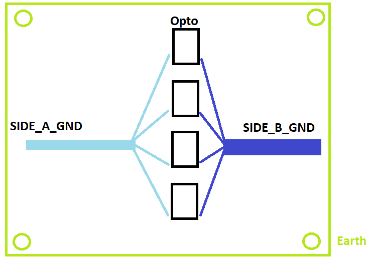
https://blog.upverter.com/2019/11/07/pcb-grounding-techniques-to-do-and-what-not-to-do/) . This is labeled as 'Earth' is the schematic (Although 'Chassis' may be a better name).
I am building a two layer PCB, but I am unsure on how to layout the copper fills for grounding:
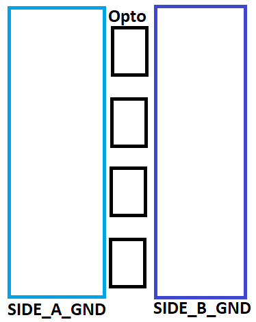
- Option A: Make a large fill on the top layer for SIDE_A_GND and a large fill on the bottom layer for SIDE_B_GND? Leave Earth unconnected.
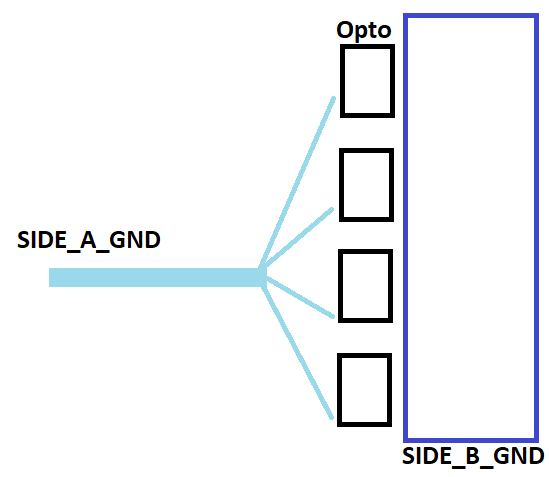
- Option B: Make two large fills in the bottom layer (one on the left for SIDE_A_GND, one on the right for SIDE_B_GND). Leave the top layer only for routing without fills. Leave Earth unconnected.

- Option C: Make large fills on both the top and bottom layer connected to SIDE_B_GND. Use a large track from the screw terminal splitting into 8 tracks towards each opto (star connection). Leave Earth unconnected.

-Option D: Use a star grounding for both SIDE_A and SIDE_B and pour fill the rest of the top/bottom of the PCB with earth.

I tried to strike a balance between providing detailed information without overflowing the post. If other important details are missing, please let me know.
Thanks a lot for any tips.
Andres
I have been googling for a while and found lots of generic advice. However, I am struggling to narrow all down to my specific case. I know this is a complicated topic, but any help would be greatly appreciated.
In the attached schematic:
- There are 8 input signals referenced to SIDE_A_GND. This is the signal side of the circuit. All inputs are 3.3VDC signals from a microcontroller. Noise immunity is very important here. Before installing the optocoupler, the power side was causing the microcontroller to reset.
- The inputs signals are isolated and boosted to 12VDC using a TLP2955. The output side of the optocouplers is referenced to SIDE_B_GND. This is the power side of the circuit. SIDE_B_GND is connected to the GND of a high power 48VDC@42A supply.
- The opto-isolated signals are used to trigger MOSFETs at 5kHz.
- I normally wire the mounting holes to a metal case to get sort of a Faraday cage (e.g. see diagram before the 'Ground Vias' header under
https://blog.upverter.com/2019/11/07/pcb-grounding-techniques-to-do-and-what-not-to-do/) . This is labeled as 'Earth' is the schematic (Although 'Chassis' may be a better name).
I am building a two layer PCB, but I am unsure on how to layout the copper fills for grounding:
- Option A: Make a large fill on the top layer for SIDE_A_GND and a large fill on the bottom layer for SIDE_B_GND? Leave Earth unconnected.
- Option B: Make two large fills in the bottom layer (one on the left for SIDE_A_GND, one on the right for SIDE_B_GND). Leave the top layer only for routing without fills. Leave Earth unconnected.
- Option C: Make large fills on both the top and bottom layer connected to SIDE_B_GND. Use a large track from the screw terminal splitting into 8 tracks towards each opto (star connection). Leave Earth unconnected.
-Option D: Use a star grounding for both SIDE_A and SIDE_B and pour fill the rest of the top/bottom of the PCB with earth.
I tried to strike a balance between providing detailed information without overflowing the post. If other important details are missing, please let me know.
Thanks a lot for any tips.
Andres