Continue to Site

Welcome to EDAboard.com

Welcome to our site! EDAboard.com is an international Electronics Discussion Forum focused on EDA software, circuits, schematics, books, theory, papers, asic, pld, 8051, DSP, Network, RF, Analog Design, PCB, Service Manuals... and a whole lot more! To participate you need to register. Registration is free. Click here to register now.

GPS receivers Front-End Design Problems

Status
Not open for further replies.

Ahmedalboshra

Junior Member level 1
Joined
Jan 15, 2020
Messages
15
Helped
0
Reputation
0
Reaction score
0
Trophy points
1
Activity points
160
I am designing a GPS L1(PWR=-160dBW) band Direct RF sampling receiver and the front-end:
(passive antenna + LNA(21dB) + BGA1(30dB) + jumper + BPF(L1(fc=1575.42MHz,BW=15MHZ) + BGA2 (30dB) + BGA3(30dB) + VGA(-13.5 to +18 Gain Control in 0.5 dB Steps) ).
all amplifiers are supplied with a +5 V power with decoupling capacitors and a test point after each component to view the signal.

The problems of the printed circuit:

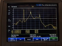
  • noise peaks through the RF line that gets amplified even though we have no input signal after each amplifier seen through the test points (+5V power is ON), no noise when +5V is OFF even when there is an input noise.
  • The BPF filters the noise peaks generated by BGA1, but the Nosie peaks still get regenerated by BGA2 .
  • One issue is that each amplifier amplifies with different GAIN values even though they are the same BGA, also I am sure I did not reach 1dB compression point(10dB).
The test point output using Network analyzer to see S-parameters ( the port1= input , port2= test points) :

  • Port2= test point after LNA:
1647005324014.jpeg
  • Port2= test point after BGA1:
1647005497307.jpeg
  • Port2= test point after BPF:
1647005567414.jpeg
  • Port2= test point after BGA2:
1647006315182.jpeg
any suggestions on the matter would really be helpful.
 

Attachments

  • 1647005846034.jpeg
    1647005846034.jpeg
    4.7 MB · Views: 113
Last edited by a moderator:

Your system is oscillating. You apply -30dBm to a system with more than 120dB Gain..
It's impossible to get a healthy result. You should apply around -110dBm ( more or less ) otherwise the amplifier will enter into saturation and they will probably oscillate.
PCB, Grounding, Decoupling, Matching etc. are extremely important.
 

Your system is oscillating. You apply -30dBm to a system with more than 120dB Gain..
It's impossible to get a healthy result. You should apply around -110dBm ( more or less ) otherwise the amplifier will enter into saturation and they will probably oscillate.
PCB, Grounding, Decoupling, Matching etc. are extremely important
thank you for replying,
I realized that the amount of amplification is a lot therefore I removed the VGA and BGA3 to just amplify with only LNA+BGA1+BGA2 which is actually the output of the screen shots I provided in thread,
when it comes to the PCB I designed 4-layer PCB (1stlayer=microstrip (50ohm matching),2ndlayer= GND,3rd layer= PWR(+5V,+3V),4thlayer=GND).
I think the circuit contains enough decoupling caps between VCC and GND.
The second test:
The input is an antenna for GPS L1 signal(L1=-160dBW) received with modified PCB(noVGA and BGA3) and these are the outputs I see in the signal using spectrum analyzer:
  • test point after LNA:
1647083827960.jpeg
  • test point after BGA1:
1647083874099.jpeg
  • test point after BPF:
1647083953346.jpeg
  • test point after BGA2:
1647084006205.jpeg
one issue I realized that each amplifier does not provide the same amount of gain even though they are the same.
 
Last edited by a moderator:

You have to do a Budget Analysis to able to see Compression of each amplifier. I still see some problems in your circuit. I cannot say a consistent word without seeing your layout and circuit.
 

May be oscillating but could also be that the sample clock or other
digital signals are spraying harmonics (seen that on a GPS RX,
cross-chip EM coupling from PLL to LNAs) or "kicking" any of the
numerous little LC tanks / stubs / radiating traces such that (to the
SpecAn) they appear as a "tone" even though they have a time
varying envelope - averaging will "stand them up" as peaks.

Bench power supplies can put out ripple and make side tones
that exceed input test power, through the supply modulation of
signal path (active or passive mixing in any / many nonlinear
elements).

Might try "stop-clock" measurement on the path, might try an
older linear supply, etc.
 

I am pretty sure your design was inspired from this one (block diagram on Fig.3):


One thing that you have to be very careful when choosing a direct sampling GPS receiver architecture, is the anti-jamming performance, mainly dictated by the wide band characteristics (you have many dB's of amplification before the BPF).

Counting all the components and many hours spent on development, I think that an already made U-blox MAX-8 would be a much better choice.
 

You have to do a Budget Analysis to able to see Compression of each amplifier. I still see some problems in your circuit. I cannot say a consistent word without seeing your layout and circuit.
This is the layout of the circuit currently I am not using any splitCombs Instead I just short circuited the RF line to BPF1 line to just use the L1 band .
The screen shots I provided are taken from the PCB that has no BGA3 and VGA.
The PCB is 4-layer PCB (1st-Layer=microstrip (50ohm matching),2nd-layer= GND,3rd-layer= PWR(+5V,+3V),4th-layer=GND).
CS = is coaxial switch for test point.
1647237239913.png
 

I am pretty sure your design was inspired from this one (block diagram on Fig.3):


One thing that you have to be very careful when choosing a direct sampling GPS receiver architecture, is the anti-jamming performance, mainly dictated by the wide band characteristics (you have many dB's of amplification before the BPF).

Counting all the components and many hours spent on development, I think that an already made U-blox MAX-8 would be a much better choice.
you are actually correct I am inspired with that paper
Therefore I am trying to make a prototype then improve on it, this is just the first prototype.
I am Just trying to learn.
If there any suggestions that could help me solve this problem I would really appreciate it .
 

Your PCB layout is huge with very long traces.
Make it 10 times smaller, and it will work much better..
 

This is the layout of the circuit currently I am not using any splitCombs Instead I just short circuited the RF line to BPF1 line to just use the L1 band .
The screen shots I provided are taken from the PCB that has no BGA3 and VGA.
The PCB is 4-layer PCB (1st-Layer=microstrip (50ohm matching),2nd-layer= GND,3rd-layer= PWR(+5V,+3V),4th-layer=GND).
CS = is coaxial switch for test point.
View attachment 174893
Your layout is not appropriate. You should use Microstrip Lines with proper width.
The jumpers cannot be used at that frequency and PCB lines are long and very thin.
Review your layout by inspiring to similar RF layouts. This is not a good layout and thin lines will reflect the signal to back and also they will act as antenna.
 

You may benefit by a system analysis. If you get into compression, amplifier will give a lower (compressed) gain. This is besides oscillation that, to me, looks still present.

For the system analysis you may use Mystic.
It is a design tool that helps you to setup and to dimension any chain made of different electronic (RF/analog) or subsystem components by calculating a bunch of performance parameters including gain, noise figure, IP3 and IM3 products at stage level.
Mystic can be used to simulate both transmitters and receivers as well as link-budgets and signal conditioning circuits.
You can easily modify the number of simulated stages without any constrains and add and remove stages at any point of the simulated signal chain.
The free version provides analysis at least of the first stage.
Here the link:

MicroWave System Calculator

Regards,
Max
 

Status
Not open for further replies.

Similar threads

Part and Inventory Search

Welcome to EDABoard.com

Sponsor

Back
Top