omdatov
Newbie level 4
Hello,
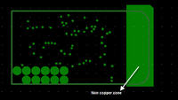
I have already posted a question, how to edit the GND plane shape of my board in order to remove a part of the GND plane. Well, I attached my gerber file and I hope that someone tell me if that's OK like this or no? I would like to know if I sent the gerber file like this, does the manufacturer will understand that the green zone means that it's a non copper zone or no?
Thanks,
I have already posted a question, how to edit the GND plane shape of my board in order to remove a part of the GND plane. Well, I attached my gerber file and I hope that someone tell me if that's OK like this or no? I would like to know if I sent the gerber file like this, does the manufacturer will understand that the green zone means that it's a non copper zone or no?

Thanks,