Continue to Site

Welcome to EDAboard.com

Welcome to our site! EDAboard.com is an international Electronics Discussion Forum focused on EDA software, circuits, schematics, books, theory, papers, asic, pld, 8051, DSP, Network, RF, Analog Design, PCB, Service Manuals... and a whole lot more! To participate you need to register. Registration is free. Click here to register now.

Gilbert Cell mixer layout

Status
Not open for further replies.

Kooky613

Member level 2
Joined
Apr 27, 2018
Messages
44
Helped
0
Reputation
0
Reaction score
1
Trophy points
8
Activity points
414
Can i implement gilbert cell in a two layer PCB? Will it work? How?
Rf freq 8 ghz
IF freq 900 MHz
 

GHz gilbert cell is primarily an IC design topic. Which discrete microwave transistor or arrays do you have available? Apart from the problem of getting suitable transistors, package parasitics will surely question the performance at 8 GHz.

As for the PCB design, having a (mostly) solid ground plane on one layer should work.
 
According to your given data, RF: 8GHz, IF: 0.9GHz, LO:8.9GHz ( or 7.1Ghz ).
For LO, you will-probably-use a discrete DRO or similar oscillator.
For IF, no problem.
The main problem I think is to find a right transistors in discrete form.The discrete transistors become day by day obsolete or not recommended for new design.
In fact it's always possible to build up a Gilbert Cell with discrete elements but the availability is the main concern.Mixers at that frequency are generally expensive and they are not available for everyone.( due export regulations ). Manufacturing Matching of the components and non ideal layout may create serious problems.
Don't try cheap FR-4 substrate, you shall have headache..
 
Thanks for the replies
FvM: The discrete transistor is from nxp (BFU910). A 2 layer layout can it work? I am asking because of the cross connections of gilbert cell.
 

Thanks for the replies
FvM: The discrete transistor is from nxp (BFU910). A 2 layer layout can it work? I am asking because of the cross connections of gilbert cell.

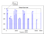
I have created a start-up design for you.You can move on it by optimizing the circuit.It's just tryout and components are ideal.No parasitic,no coupling,no layout.
Conversion Gain : 5.5dB (approx.)

Q1..Q6: BFP405F
RB1:87k
RB2:110k
Ic(Q1..Q4):5mA
Ic(Q5,Q6):10mA
RL:50 Ohm

8GHz_GC.png

8GHz_GC_spectrum.png

8GHz_GC_core.png
 
Last edited:
BigBoss thanks for the reply
I have already a scematic with distributed elements..
And i want to know if it can be implemented on a 2 layer becayse of the cross points
 

What calculations do i need to do? i do not understand...
 

Yes but i do not know what to do with the cross connections
 

Means sketch the layout, see how it goes.

- - - Updated - - -

1. There's still room between the pins
2. You may consider a few short jumper routes on the bottom layer
 

Status
Not open for further replies.

Part and Inventory Search

Welcome to EDABoard.com

Sponsor

Back
Top