Welcome to our site! EDAboard.com is an international Electronics Discussion Forum focused on EDA software, circuits, schematics, books, theory, papers, asic, pld, 8051, DSP, Network, RF, Analog Design, PCB, Service Manuals... and a whole lot more! To participate you need to register. Registration is free. Click here to register now.
Gate driver design driving two different transistors in each half cycle
Hi all,
Can you help me in designing a gate driver circuit which drives one transistor in half period and other transistor in rest. Design is in AMI 0.5um process.
Depends if you need non-overlapping clocks or not. If not, you could simply use the same clock signal for both transistors (like in a normal inverter). If the two transistors are connected in series, however - like in a normal inverter - you'll get current shot through during switching, what might not be important for a small inverter, but with such wide transistors could short circuit your power supply or even destroy the transistors. In such case you'd need to use non-overlapping clocks.
Hi Erikl!
Thanks for replying to my question. I have two transistors in different blocks which have to be switched at same time. But, after you said, I understood that I need two independent drivers for each of the transistor. Can you help me how I can design two driver circuits driving two different transistors in two different blocks switch at same time. I am not sure how to start with the design.
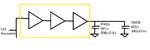
I considered like the following, please correct me if I am wrong,
Cout=W*L*1.5*2.4fF/um2
Let W=685um, L=0.6u
Cout= 1.477pF
Cin of INVX1=C from PMOS + C from NMOS
Cin of INVX1=(3u*0.6u*1.5*2.4fF/um2)+ (1.5u*0.6u*1.5*2.4fF/um2)
Cin of INVX1=9.72fF
H=Cout/Cin=1.477p/9.72f= 151.44
N=ln(H)= 5, Number of stages= 5
Scale factor= H^(1/N)= 151^(1/5)= 2.72~3
But scale factor of 3 is said be not good, as it is either power loss or slow.
The 5 stages look like 1:3:7:20:55
I have two transistors in different blocks which have to be switched at same time. ... I understood that I need two independent drivers for each of the transistor.
If I understand correctly, both transistors should be "on" (and "off") at the same time? So you need only one driver chain, and one big inverter for the other transistor.
I think 3 inverters (for the inverted signal) and one more inverter (for the non-inverted signal) should be enough for the tapering,
s. e.g. Craig Prunty and Laszlo Gal "Optimum Tapered Buffer", IEEE JOURNAL OF SOLID-STATE CIRCUITS, VOL. 27, NO. 1, JANUARY 1992, p. 118-119.
Pls. read my answer thoroughly: I think 3 resp. 4 inverters are enough. A scale factor of 3 isn't necessary; a factor of 4..5 is sufficient.
Run transient analyses and compare!
This site uses cookies to help personalise content, tailor your experience and to keep you logged in if you register.
By continuing to use this site, you are consenting to our use of cookies.