Continue to Site

Welcome to EDAboard.com

Welcome to our site! EDAboard.com is an international Electronics Discussion Forum focused on EDA software, circuits, schematics, books, theory, papers, asic, pld, 8051, DSP, Network, RF, Analog Design, PCB, Service Manuals... and a whole lot more! To participate you need to register. Registration is free. Click here to register now.

gate driver and protection circuit for IGBT.

Status
Not open for further replies.

aliraza786

Full Member level 4
Joined
Nov 10, 2009
Messages
210
Helped
14
Reputation
28
Reaction score
14
Trophy points
1,298
Location
Lahore, Pakistan, Pakistan
Activity points
2,914
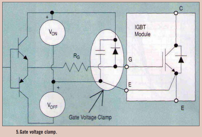
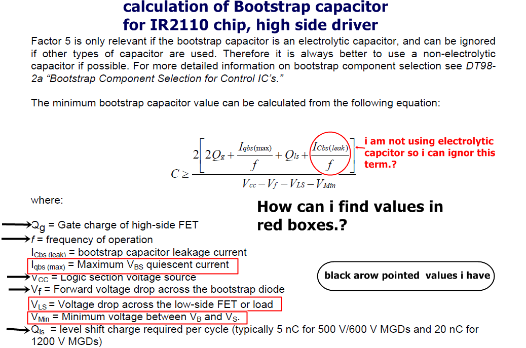
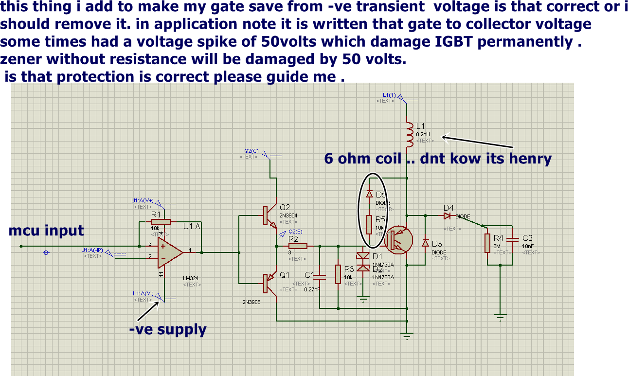
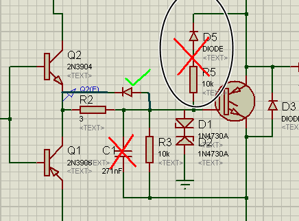
i am using 80N60 IGBT to drive my inductive load of resistance 6ohm.. i use 4N25 optocoupler to drive gate i use 20 volts supply for gate... system voltage is 300volts DC .. i give a pulse at the gate of IGBT for 100ms just... my circuit works great but after almost 1.5 day IGBT burnt now it collector and emitter is shorted internally...i use snubber circuit and free wheeling diode to protect .. but again IGBT fails... kindly guide me how can i improve my gate driver and protection circuitry thanks :)
 

Hi aliraza,
For driving the IGBT it is better to use IR2110 it can work upto 500v on the high side. is your load a motor if so then you should incorporate soft start in circuit. datasheet attached.
regards ani
 

Attachments

  • ir2110.pdf
    210.3 KB · Views: 233
Does the IGBT overheat before being damaged? Was the circuit running for the entire 1.5 days?

In general, for protection, a gate to emitter resistor in parallel with a zener could be used.
 

thanks for suggestion picgak i decided to use your suggested chip :)
tahmid sir i am waiting for you... thanks for your response... i just switch it for 100ms so it doesn't heat.. when it proper functioning.. i switch it many times in 1.5 days ... not all the time... and one more thing i decided to use IR2110 chip many people said it is very difficult to drive currently i am studying application notes. can i use single high side driver for my circuit.? i thing high side driver is better for inductive loads..

what about this circuit i find it on net.. what is the use of clamp circuit.? it that a better circuit to drive it.?

- - - Updated - - -

kindly help me in calculating IR2110 boot straping capacitor ..
 
Hi aliraza,
My knowledge in theory is limited i am more attached to practical,I think Mr Tahmid can guide you better in theory, any way i am attaching another datasheet hope it may solve your bootstrap capacitor problem. if you can post the the circuit used in the igbt driver stage you used earlier we can find the solution for that.
regards ani
 

Attachments

  • dt04-4.pdf
    607.2 KB · Views: 178
  • HV Floating MOS-Gate Driver ICs.pdf
    240.6 KB · Views: 231
Last edited:

The said application has been presented as low side switch in parallel threads and thus won't use bootstrap...

IR2110 can be still used as a low side switch.
 
You can use low-side driving as well. It shouldn't be a problem. And you don't need high-side bootstrapped driving either.

Check the voltage across the IGBT using an oscilloscope while the IGBT is running. Observe any spikes and record how large the spikes are.

Have you used a free-wheeling diode ACROSS THE LOAD?
 
yeah Tahmid sir i use free wheeling diode and snubber. and that circuit i posted what you think about it ... is it a better drive circuit.? ok i do experiment with Oscilloscope ... thanks for your suggestion..
 

Hi aliraza,
where is your original circuit? we can find what is wrong in it.
Regards ani
 
There are obvious drawing faults and many unclear points. I fear it's impossible to discuss the present version, because we don't know what's real.

- Q1 connected wrong
- connection of driver ground to IGBT emitter is missing
- C1 has a "ridiculous" high value, what's the purpose of C1 at all?
- R5/D5 can't be related to any usual IGBT driver scheme, please clarify
- L1 value can't be real

Regarding your comment, I don't understand about "gate-to-collector" voltage peak. IGBTs are usually damaged by violating Vge (20 to 30 V) or Vce (e.g. 1200 V) rating.

sir i have read in application note of some company in which they place capacitor at input which value depend on the input capacitance of IGBT.. my IGBT has input capacitance of 2800pf thats why i place 28pf capcitor which is 10% of input capacitance .. they write there this capcitor is to avoid the stray inductance. and in the same paper they said gate to collector voltage spike can damage IGBT so i place zener head to head to save the gate (they do not place R5 and D5 ) . but if we apply 50 volts at the zener which is used to regulate 15 volts then it will burn there must be some reistance.. thats why i place D5 and R5 .D5 will conduct in -ve Transient so resistance will come in the path so voltage drop across it and zener remain safe. m confused about this part R5 and D5.. becuse this is my own thinking . previous values are not real but now it is actual on
 

Hi aliraza,
If you use C1 it will prevent switching on & off immediately with respect to the incomming pulse and lead to failures. D5, R5 is also wrong. you can use a diode as shown below to fastly remove charge from the gate while swthing off the IGBT
regards ani
30_1347013010.png
 

28 pF is somehow different from "271nF" as printed in the previous post. In case you want additional capacitance, the transil diode is bringing more than necessary. But don't want to argue about 28 pF.

Inductance of L1 is a point you should be worried about. If it's larger than a few µH, the stored energy at 50 A will blow the IGBT. If slower decay of load current isn't an issue, you'll better place a reverse diode across L1.
 

Status
Not open for further replies.

Similar threads

Part and Inventory Search

Welcome to EDABoard.com

Sponsor

Back
Top