Continue to Site

Welcome to EDAboard.com

Welcome to our site! EDAboard.com is an international Electronics Discussion Forum focused on EDA software, circuits, schematics, books, theory, papers, asic, pld, 8051, DSP, Network, RF, Analog Design, PCB, Service Manuals... and a whole lot more! To participate you need to register. Registration is free. Click here to register now.

Full wave rectifier (familiar circuit)

Status
Not open for further replies.

Yair Malka

Newbie level 2
Joined
May 14, 2014
Messages
2
Helped
0
Reputation
0
Reaction score
0
Trophy points
1
Activity points
20
Hey, I'm new here.
My English is't good enough so I apologize about the Grammer mistakes.

I have some mini-work to do about the Full wave rectifier.
The work is to explain the behaviour of the circuit.
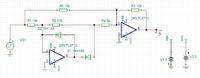
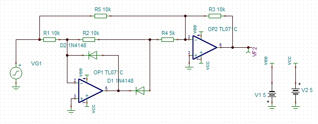
The circuit looks like that:


I just want to know how does the circuit work?
maybe more important how does the 1st amplifier works?
I ran a simulation in Tina (software) and got this behaviour for the first stage:


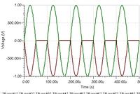
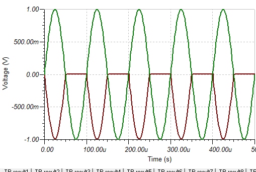
If i will know how the first stage works, and why in the positive wave input I get a negative wave at the output,
and when the input is negative I get zero at the output, I will understand properly how the circuit works because I know how the second stage works.
I will really glad to know how it works and especially the first stage (with the two diodes).
Thank you very much, and sory about the English again.
 

I can't see the attachments.
 

try this java applet simulator

bridge.jpg
 

The opamps are TL071 that have a minimum total supply voltage of 7V but your circuit has a total of only 4V so it will not work!

It should be obvious that the opamps are inverting so of course with a positive input then the output of the first opamp is negative then the output of the second opamp is positive. When the input is negative then the output of the second opamp again is positive.
 

The opamps are TL071 that have a minimum total supply voltage of 7V but your circuit has a total of only 4V so it will not work!
I can see +5V, -5V so the total supply is 10V.

However the first stage (R1, R2, D1, D2, OP1) works this way:

If the input is positive, due to the inverting configuration, the output of the op-amp will be negative then the diode D1 will be reverse polarized (cathode more positive than anode); the diode D2 will be instead directly polarized because the voltage between R2 and R4 is less than that between R1 and R2. You can imagine the diodes as two switches: D1 open and D2 closed. This means under this condition the circuit will behaves as an inverting amplifier with gain R2/R1 (that is G=1 in our case)

If the input is negative, instead, the output will be positive then now the diode D1 will be directly polarized while D2 will be reverse polarized. Using again the switches approximation, D1 will be a switch closed while D2 will be open. This means the output of the op-amp will result "floating" with respect to the rest of the circuit, then the output of R2 will be zero because it will se the ground through the virtual ground seen at the inverting input of OP1.

Thank you Very much!
You really helped me to understand it!
 

Status
Not open for further replies.

Part and Inventory Search

Welcome to EDABoard.com

Sponsor

Back
Top