adezie
Newbie level 4
greetings, I have built an H-Bridge circuit and using IR2113 to drive the high and low side, I've created an SPWM lookup table for my microcontroller to feed SPWM signals to LIN and HIN, here's the signal,
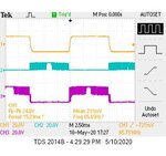
 blue is HIGH side MOSFET gate signal and yellow is LOW side MOSFET gate signal, Vgs of the HIGH side of MOSFET without VDC applied, but when I attached 12VDC, here's the signal
  purple is the output and its not Sine wave, there is no problem at bootstrapping since the VGS at high side always got 12V, what do I mess with ? is it the circuit ? or the PWM ? or what? I need advice so bad, here's the IR2113 layout
here's the lookup table
here's the setup in my microcontroller
blue is HIGH side MOSFET gate signal and yellow is LOW side MOSFET gate signal, Vgs of the HIGH side of MOSFET without VDC applied, but when I attached 12VDC, here's the signal purple is the output and its not Sine wave, there is no problem at bootstrapping since the VGS at high side always got 12V, what do I mess with ? is it the circuit ? or the PWM ? or what? I need advice so bad, here's the IR2113 layout here's the lookup table
Code:
int sine[] = {
  31.41552779, 31.41552779, 62.82866317, 94.23701391, 125.6381881, 157.0297945, 188.4094425, 219.7747423, 251.1233055, 282.4527446, 313.7606739, 345.0447091, 376.3024678, 407.5315696, 438.7296363, 469.894292,
  501.0231635, 532.1138801, 563.1640741, 594.1713811, 625.1334396, 656.0478918, 686.9123834, 717.7245639, 748.4820869, 779.1826102, 809.8237956, 840.4033099, 870.9188242, 901.3680146, 931.7485624,
  962.0581539, 992.2944809, 1022.455241, 1052.538137, 1082.540878, 1112.46118, 1142.296763, 1172.045356, 1201.704693, 1231.272516, 1260.746573, 1290.124618, 1319.404416, 1348.583736, 1377.660357,
  1406.632063, 1435.496648, 1464.251915, 1492.895674, 1521.425742, 1549.839949, 1578.136128, 1606.312127, 1634.365799, 1662.295008, 1690.097626, 1717.771537, 1745.314633, 1772.724816, 1800, 1827.138107,
  1854.13707, 1880.994833, 1907.709351, 1934.27859, 1960.700526, 1986.973147, 2013.094452, 2039.062453, 2064.875171, 2090.530641, 2116.026908, 2141.362032, 2166.534083, 2191.541144, 2216.381311,
  2241.052692, 2265.553408, 2289.881593, 2314.035395, 2338.012974, 2361.812504, 2385.432174, 2408.870183, 2432.124747, 2455.194096, 2478.076472, 2500.770134, 2523.273351, 2545.584412, 2567.701617,
  2589.623281, 2611.347736, 2632.873326, 2654.198413, 2675.321372, 2696.240595, 2716.954489, 2737.461476, 2757.759995, 2777.8485, 2797.725461, 2817.389365, 2836.838713, 2856.072025, 2875.087836,
  2893.884698, 2912.46118, 2930.815866, 2948.947359, 2966.854279, 2984.535261, 3001.988959, 3019.214045, 3036.209205, 3052.973146, 3069.504592, 3085.802283, 3101.864978, 3117.691454, 3133.280505,
  3148.630946, 3163.741606, 3178.611334, 3193.238999, 3207.623487, 3221.763702, 3235.658567, 3249.307024, 3262.708033, 3275.860575, 3288.763648, 3301.416268, 3313.817472, 3325.966317, 3337.861876,
  3349.503245, 3360.889535, 3372.019881, 3382.893435, 3393.509368, 3403.866872, 3403.866872, 3393.509368, 3382.893435, 3372.019881, 3360.889535, 3349.503245, 3337.861876, 3325.966317, 3313.817472, 3301.416268,
  3288.763648, 3275.860575, 3262.708033, 3249.307024, 3235.658567, 3221.763702, 3207.623487, 3193.238999, 3178.611334, 3163.741606, 3148.630946, 3133.280505, 3117.691454, 3101.864978, 3085.802283,
  3069.504592, 3052.973146, 3036.209205, 3019.214045, 3001.988959, 2984.535261, 2966.854279, 2948.947359, 2930.815866, 2912.46118, 2893.884698, 2875.087836, 2856.072025, 2836.838713, 2817.389365,
  2797.725461, 2777.8485, 2757.759995, 2737.461476, 2716.954489, 2696.240595, 2675.321372, 2654.198413, 2632.873326, 2611.347736, 2589.623281, 2567.701617, 2545.584412, 2523.273351, 2500.770134,
  2478.076472, 2455.194096, 2432.124747, 2408.870183, 2385.432174, 2361.812504, 2338.012974, 2314.035395, 2289.881593, 2265.553408, 2241.052692, 2216.381311, 2191.541144, 2166.534083, 2141.362032,
  2116.026908, 2090.530641, 2064.875171, 2039.062453, 2013.094452, 1986.973147, 1960.700526, 1934.27859, 1907.709351, 1880.994833, 1854.13707, 1827.138107, 1800, 1772.724816, 1745.314633, 1717.771537,
  1690.097626, 1662.295008, 1634.365799, 1606.312127, 1578.136128, 1549.839949, 1521.425742, 1492.895674, 1464.251915, 1435.496648, 1406.632063, 1377.660357, 1348.583736, 1319.404416, 1290.124618,
  1260.746573, 1231.272516, 1201.704693, 1172.045356, 1142.296763, 1112.46118, 1082.540878, 1052.538137, 1022.455241, 992.2944809, 962.0581539, 931.7485624, 901.3680146, 870.9188242, 840.4033099,
  809.8237956, 779.1826102, 748.4820869, 717.7245639, 686.9123834, 656.0478918, 625.1334396, 594.1713811, 563.1640741, 532.1138801, 501.0231635, 469.894292, 438.7296363, 407.5315696, 376.3024678,
  345.0447091, 313.7606739, 282.4527446, 251.1233055, 219.7747423, 188.4094425, 157.0297945, 125.6381881, 94.23701391, 62.82866317, 31.41552779, 31.41552779


};
Code:
HardwareTimer timerA(3);
a=1;
char H1 = PB0;
char L1 = PB1;
void setup() {
  Serial1.begin(9600);
  //  pinMode(PA9, OUTPUT_OPEN_DRAIN);
  pinMode(H1, PWM_OPEN_DRAIN);//H1
  pinMode(L1, PWM_OPEN_DRAIN);//L1
  pinMode(PA1, INPUT);//Vac
  pinMode(PA7, INPUT_ANALOG);//Vdc
  pinMode(PA3, INPUT_ANALOG);//Iout
  timerA.setPrescaleFactor(1);
  timerA.setOverflow(3600);

}

Void Loop(){
  for (int i = 0; i < 20; i++) {
    pwmWrite(H1, (3600 - sine[i])*a);
    pwmWrite(L1, 3600);
  }
  for (int i = 20; i < 267; i++) {
    pwmWrite(H1, (3600 - sine[i])*a);
    pwmWrite(L1, 3600);
    delayMicroseconds(W);
  }
  for (int i = 267; i < 287; i++) {
    pwmWrite(H1, (3600 - sine[i])*a);
    pwmWrite(L1, 3600);
  }
  for (int i = 0; i < 20; i++) {
    pwmWrite(L1, (3600 - sine[i])*a);
    pwmWrite(H1, 3600);
  }
  for (int i = 20; i < 267; i++) {
    pwmWrite(L1, (3600 - sine[i])*a);
    pwmWrite(H1, 3600);
    delayMicroseconds(W);
  }
  for (int i = 267; i < 287; i++) {
    pwmWrite(L1, (3600 - sine[i])*a);
    pwmWrite(H1, 3600);
  }
}
Attachments
Last edited by a moderator:
